- 您現(xiàn)在的位置:買賣IC網(wǎng) > PDF目錄98252 > TLV320AIC13I (TEXAS INSTRUMENTS INC) SPECIALTY CONSUMER CIRCUIT, PDSO30 PDF資料下載
參數(shù)資料
| 型號: | TLV320AIC13I |
| 廠商: | TEXAS INSTRUMENTS INC |
| 元件分類: | 消費家電 |
| 英文描述: | SPECIALTY CONSUMER CIRCUIT, PDSO30 |
| 封裝: | PLASTIC, SOP-30 |
| 文件頁數(shù): | 5/55頁 |
| 文件大?。?/td> | 455K |
| 代理商: | TLV320AIC13I |
第1頁第2頁第3頁第4頁當(dāng)前第5頁第6頁第7頁第8頁第9頁第10頁第11頁第12頁第13頁第14頁第15頁第16頁第17頁第18頁第19頁第20頁第21頁第22頁第23頁第24頁第25頁第26頁第27頁第28頁第29頁第30頁第31頁第32頁第33頁第34頁第35頁第36頁第37頁第38頁第39頁第40頁第41頁第42頁第43頁第44頁第45頁第46頁第47頁第48頁第49頁第50頁第51頁第52頁第53頁第54頁第55頁

2–2
2.2
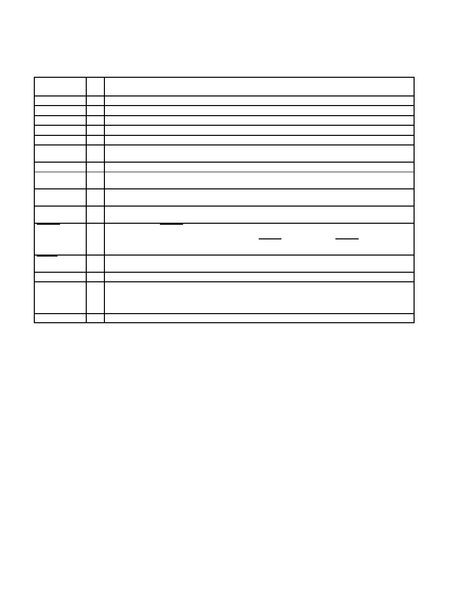
Terminal Functions (Continued)
TERMINAL
I/O
DESCRIPTION
NAME
NO.
I/O
DESCRIPTION
IOVDD
2
I
Digital I/O power supply
IOVSS
1
I
Digital I/O ground
MCLK
25
I
Master clock. MCLK derives the internal clocks of the sigma-delta analog interface circuit.
MICIN
18
I
MIC preamplifier input. It must be connected to AVSS if not used.
M/S
7
I
Master/slave select input. When M/S is high, the device is the master, and when low it is a slave.
OUTM1
9
O
Inverting output of the DAC. OUTM1 is functionally identical with and complementary to OUTP1. This differential
output can drive a minimum load of 600
. This output can also be used alone for single-ended operation.
OUTMV
14
O
Programmable virtual ground for the output of OUTP2 and OUTP3 (see Register Map).
OUTP1
10
O
Noninverting output of the DAC. This differential output can drive a minimum load of 600
. This output can also be
used alone for single-ended operation.
OUTP2
13
O
Analog output #2 from the 16-
driver. This output can drive a minimum load of 16 and also can be configured as
either single-ended output or differential output by the control register 6.
OUTP3
15
O
Analog output #3 from the 16-
driver. This output can drive a minimum load of 16 and also be configured as either
single-ended output or differential output by the control register 6.
PWRDN
8
I
Power down. When PWRDN is pulled low, the device goes into a power-down mode, the serial interface is disabled,
and most of the high-speed clocks are disabled. However, all the register values are sustained and the device
resumes full-power operation without reinitialization when PWRDN is pulled high again. PWRDN resets the counters
only and preserves the programmed register contents.
RESET
24
I
Hardware reset. The reset function is provided to initialize all of the internal registers to their default values. The serial
port is configured to the default state accordingly.
SCL
26
I
Programmable host port (I2C or S2C) clock input.
SCLK
28
I/O
Shift clock. SCLK signal clocks serial data into DIN and out of DOUT during the frame-sync interval. When configured
as an output (M/S high), SCLK is generated internally by multiplying the frame-sync signal frequency by 16 and the
number of codecs in cascade in standard and continuous mode. When configured as an input (M/S low), SCLK is
generated externally and must be synchronous with the master clock and frame sync.
SDA
27
I/O
Programmable host port (I2C or S2C) data line.
2.3
Definitions and Terminology
Data Transfer
Interval
The time during which data is transferred from DOUT and to DIN. The interval is 16 shift clocks and the data
transfer is initiated by the falling edge of the FS signal in standard and continuous mode.
Signal Data
This refers to the input signal and all of the converted representations through the ADC channel and the
signal through the DAC channel to the analog output. This is contrasted with the purely digital software
control data.
Frame Sync
Frame sync refers only to the falling edge of the signal FS that initiates the data transfer interval
Frame Sync and
Sampling Period
Frame sync and sampling period is the time between falling edges of successive FS signals.
fs
The sampling frequency
ADC Channel
ADC channel refers to all signal processing circuits between the analog input and the digital
conversion result at DOUT.
DAC channel
DAC channel refers to all signal processing circuits between the digital data word applied to DIN and the
differential output analog signal available at OUTP1and OUTM.
Dxx
Bit position in the primary data word (xx is the bit number)
DSxx
Bit position in the secondary data word (xx is the bit number)
PGA
Programmable gain amplifier
IIR
Infinite impulse response
FIR
Finite impulse response
相關(guān)PDF資料 |
PDF描述 |
|---|---|
| TLV320AIC14C | SPECIALTY CONSUMER CIRCUIT, PDSO30 |
| TLV320AIC14I | SPECIALTY CONSUMER CIRCUIT, PDSO30 |
| TLV320AIC22PT | SPECIALTY CONSUMER CIRCUIT, PQFP48 |
| TLV320AIC22PTR | SPECIALTY CONSUMER CIRCUIT, PQFP48 |
| TLV320AIC23BGQE | SPECIALTY CONSUMER CIRCUIT, PBGA80 |
相關(guān)代理商/技術(shù)參數(shù) |
參數(shù)描述 |
|---|---|
| TLV320AIC13IDBT | 功能描述:接口—CODEC Lo-Pwr Mono Voice Band CODEC RoHS:否 制造商:Texas Instruments 類型: 分辨率: 轉(zhuǎn)換速率:48 kSPs 接口類型:I2C ADC 數(shù)量:2 DAC 數(shù)量:4 工作電源電壓:1.8 V, 2.1 V, 2.3 V to 5.5 V 最大工作溫度:+ 85 C 安裝風(fēng)格:SMD/SMT 封裝 / 箱體:DSBGA-81 封裝:Reel |
| TLV320AIC13IDBTG4 | 功能描述:接口—CODEC Lo-Pwr Mono Voice Band CODEC RoHS:否 制造商:Texas Instruments 類型: 分辨率: 轉(zhuǎn)換速率:48 kSPs 接口類型:I2C ADC 數(shù)量:2 DAC 數(shù)量:4 工作電源電壓:1.8 V, 2.1 V, 2.3 V to 5.5 V 最大工作溫度:+ 85 C 安裝風(fēng)格:SMD/SMT 封裝 / 箱體:DSBGA-81 封裝:Reel |
| TLV320AIC13IDBTR | 功能描述:接口—CODEC Lo-Pwr Mono Voice Band CODEC RoHS:否 制造商:Texas Instruments 類型: 分辨率: 轉(zhuǎn)換速率:48 kSPs 接口類型:I2C ADC 數(shù)量:2 DAC 數(shù)量:4 工作電源電壓:1.8 V, 2.1 V, 2.3 V to 5.5 V 最大工作溫度:+ 85 C 安裝風(fēng)格:SMD/SMT 封裝 / 箱體:DSBGA-81 封裝:Reel |
| TLV320AIC13IDBTRG4 | 功能描述:接口—CODEC Lo-Pwr Mono Voice Band CODEC RoHS:否 制造商:Texas Instruments 類型: 分辨率: 轉(zhuǎn)換速率:48 kSPs 接口類型:I2C ADC 數(shù)量:2 DAC 數(shù)量:4 工作電源電壓:1.8 V, 2.1 V, 2.3 V to 5.5 V 最大工作溫度:+ 85 C 安裝風(fēng)格:SMD/SMT 封裝 / 箱體:DSBGA-81 封裝:Reel |
| TLV320AIC14 | 制造商:TI 制造商全稱:Texas Instruments 功能描述:LOW-POWER, HIGHLY-INTEGRATED, PROGRAMMABLE 16-Bit, 26-KSPS MONO CODEC |
發(fā)布緊急采購,3分鐘左右您將得到回復(fù)。