- 您現(xiàn)在的位置:買賣IC網(wǎng) > PDF目錄359354 > VDP3130Y (MICRONAS SEMICONDUCTOR HOLDING AG) Video Processor Family PDF資料下載
參數(shù)資料
| 型號: | VDP3130Y |
| 廠商: | MICRONAS SEMICONDUCTOR HOLDING AG |
| 英文描述: | Video Processor Family |
| 中文描述: | 視頻處理器系列 |
| 文件頁數(shù): | 56/76頁 |
| 文件大小: | 1770K |
| 代理商: | VDP3130Y |
第1頁第2頁第3頁第4頁第5頁第6頁第7頁第8頁第9頁第10頁第11頁第12頁第13頁第14頁第15頁第16頁第17頁第18頁第19頁第20頁第21頁第22頁第23頁第24頁第25頁第26頁第27頁第28頁第29頁第30頁第31頁第32頁第33頁第34頁第35頁第36頁第37頁第38頁第39頁第40頁第41頁第42頁第43頁第44頁第45頁第46頁第47頁第48頁第49頁第50頁第51頁第52頁第53頁第54頁第55頁當前第56頁第57頁第58頁第59頁第60頁第61頁第62頁第63頁第64頁第65頁第66頁第67頁第68頁第69頁第70頁第71頁第72頁第73頁第74頁第75頁第76頁
VDP 313xY
ADVANCE INFORMATION
56
Micronas
Pin 37, 38, 39
Analog RGB Outputs,
ROUT, GOUT,
BOUT
(Fig. 3
–
12)
This are the analog Red/Green/Blue outputs of the
backend. The outputs sink a current of max. 8 mA.
Pin 40
DAC Reference Decoupling,
VRD
(Fig. 3
–
20)
Via this pin the DAC reference voltage is decoupled by
an external capacitance. The DAC output currents
depend on this voltage, therefore a pull-down transis-
tor can be used to shut off all beam currents. A decou-
pling capacitor of 3.3
μ
F/100 nF is required.
Pin 41, 42, 43, 45, 46, 47
Analog RGB Inputs,
RIN1/
2, GIN1/2, BIN1/2
(Fig. 3
–
11)
These pins are used to insert an external analog RGB
signal, e.g. from a SCART connector which can by
switched to the analog RGB outputs with the fast blank
signal. The analog backend provides separate bright-
ness and contrast settings for the external analog RGB
signals.
Pin 44, 48
Fast Blank Inputs,
FBLIN1/2
(Fig. 3
–
15)
These pins are used to switch the RGB outputs to the
external analog RGB inputs.
Pin 49
Main Clock Output,
CLK20
( Fig. 3
–
6)
This is the 20.25 MHz main system clock, that is used
by all circuits in a high-end VDP system. All external
timing is derived from this clock.
Pin 50
Horizontal Drive Output,
HOUT
(Fig. 3
–
13)
This open drain output supplies the the drive pulse for
the horizontal output stage. The polarity and gating
with the flyback pulse are selectable by software.
Pin 51, 52
Crystal Input and Output,
XTAL1
,
XTAL2
(Fig. 3
–
5)
These pins are connected to an 20.25 MHz crystal
oscillator is digitally tuned by integrated shunt capaci-
tances. The Clk20 signal is derived from this oscillator.
Pin 53, 54, 60
Analog Chroma Inputs,
CIN1, CIN2/
CRIN, CBIN
,
(Fig. 3
–
7, Fig. 3
–
8)
CIN1, CIN2 are the analog chroma inputs for S-VHS. A
S-VHS chroma signal is converted using the chroma
(Video2) AD converter. A resistive devider is used to
BIAS the inout signal to middle of converter range. The
input signal must be AC coupled. Together with the
CBIN pin CIN2 can alternatively be used as chroma
component input for the analog YC
R
C
B
interface.
Pin 55
Ground (Analog Front-end),
GNDAF
Pin 56
Ground (Analog Signal Input),
SGND
(Fig. 3
–
10)
This is the high quality ground reference for the video
input signals.
Pin 57
Reference Voltage Top,
VRT
(Fig. 3
–
10)
Via this pin, the reference voltage for the A/D convert-
ers is decoupled. The pin is connected with 10
μ
F/
47 nF to the Signal Ground Pin.
Pin 58
Supply Voltage (Analog Front-end),
VSUPAF
Pin 59
Analog Video Output,
VOUT
(Fig. 3
–
9)
The analog video signal that is selected for the main
(luma, cvbs) adc is output at this pin. An emitter fol-
lower is required at this pin.
Pin 61...64
Analog Video Input 1
4,
VIN1
4
(Fig. 3
–
7)
These are the analog video inputs. A CVBS or S-VHS
luma signal is converted using the luma (Video 1) AD
converter. The input signal must be AC-coupled.
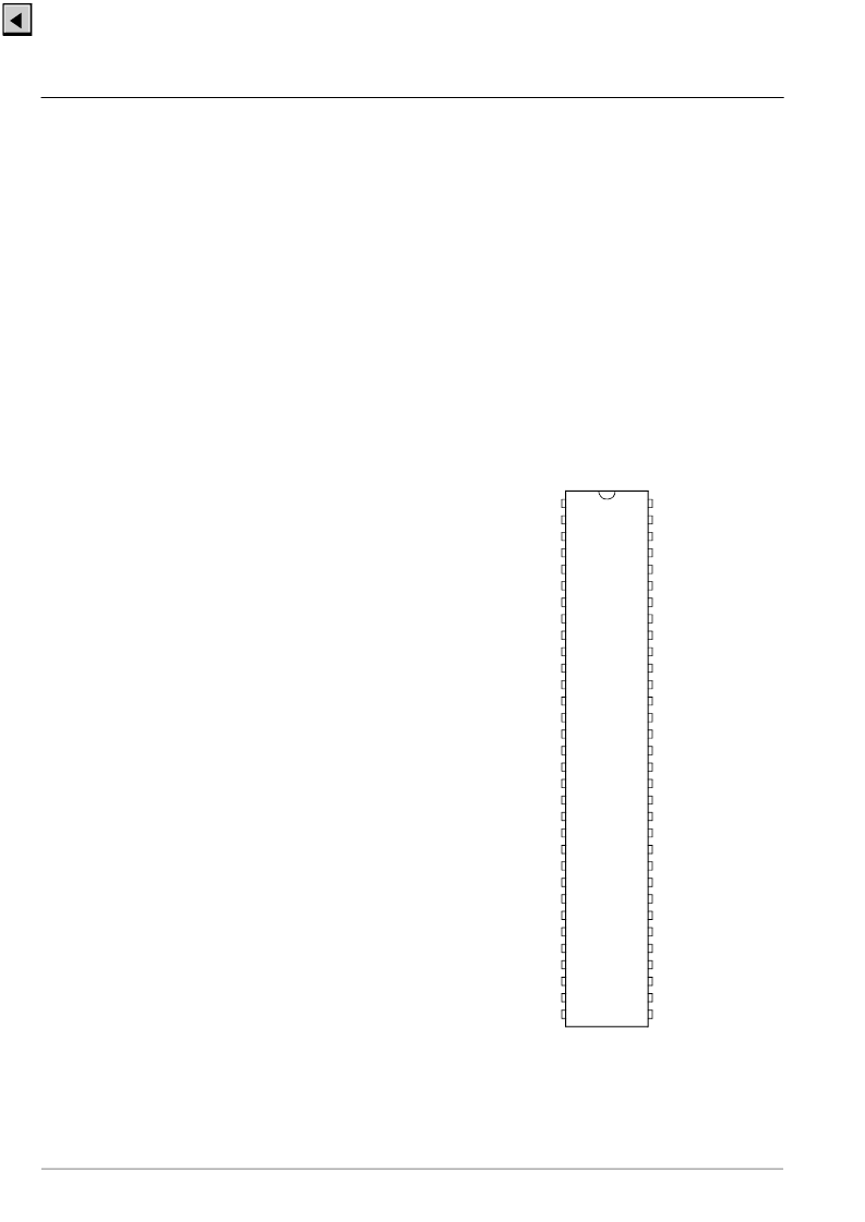
3.4. Pin Configuration
Fig. 3
–
2:
64-pin PSDIP package
1
2
3
4
5
6
7
8
9
10
11
12
13
14
15
16
17
18
19
20
21
22
23
24
25
26
27
28
29
30
31
32
TEST
RESQ
SCL
SDA
GNDD
HCS
FSY
CSY
VS
INTLC
VPROT
SAFETY
HFLB
GNDD
VSUPD
GNDD
VSUPD
VIN4
VIN3
VIN2
VIN1
CIN1
VOUT
VSUPAF
VRT
SGND
GNDAF
CBIN
CIN 2/CRIN
XTAL 2
XTAL 1
HOUT
CLK20
FBLIN2
BIN2
GIN2
RIN2
FBLIN
BIN
GIN
RIN
VRD
BOUT
GOUT
ROUT
VSUPAB
GNDAB
SVMOUT
XREF
64
63
62
61
60
59
58
57
56
55
54
53
52
51
50
49
48
47
46
45
44
43
42
41
40
39
38
37
36
35
34
33
P0
P1
P2
P3
P4
P5
P6
GNDD
RSW2
RSW1
SENSE
GNDM
VERTQ
VERT
E/W
V
相關(guān)PDF資料 |
PDF描述 |
|---|---|
| VDP31XXB | Video Processor Family |
| VDP3108PR | Consumer IC |
| VDSGLD_38.88 | TRANS PREBIASED PNP 200MW SOT23 |
| VDSL5100I | TVS 400W 43V UNIDIRECT SMA |
| VDSL5100 | TVS 400W 40V BIDIRECT SMA |
相關(guān)代理商/技術(shù)參數(shù) |
參數(shù)描述 |
|---|---|
| VDP3131Y | 制造商:MICRONAS 制造商全稱:MICRONAS 功能描述:Video Processor Family |
| VDP3132Y | 制造商:MICRONAS 制造商全稱:MICRONAS 功能描述:Video Processor Family |
| VDP3133Y | 制造商:MICRONAS 制造商全稱:MICRONAS 功能描述:Video Processor Family |
| VDP3134Y | 制造商:MICRONAS 制造商全稱:MICRONAS 功能描述:Video Processor Family |
| VDP313XY | 制造商:MICRONAS 制造商全稱:MICRONAS 功能描述:Video Processor Family |
發(fā)布緊急采購,3分鐘左右您將得到回復。