- 您現(xiàn)在的位置:買(mǎi)賣(mài)IC網(wǎng) > PDF目錄361772 > W229B Clocks and Buffers PDF資料下載
參數(shù)資料
| 型號(hào): | W229B |
| 英文描述: | Clocks and Buffers |
| 中文描述: | 時(shí)鐘和緩沖器 |
| 文件頁(yè)數(shù): | 3/17頁(yè) |
| 文件大小: | 183K |
| 代理商: | W229B |
第1頁(yè)第2頁(yè)當(dāng)前第3頁(yè)第4頁(yè)第5頁(yè)第6頁(yè)第7頁(yè)第8頁(yè)第9頁(yè)第10頁(yè)第11頁(yè)第12頁(yè)第13頁(yè)第14頁(yè)第15頁(yè)第16頁(yè)第17頁(yè)
W229B
Document #: 38-07223 Rev. *A
Page 3 of 17
Overview
The W229B is a highly integrated frequency timing generator,
supplying all the required clock sources for an Intel
architec-
ture platform using graphics integrated core logic.
Functional Description
I/O Pin Operation
Pin # 3, 11, 12, 13, 23, and 24 are dual-purpose l/O pins. Upon
power-up the pin acts as a logic input. An external 10-k
strap-
ping resistor should be used.
Figure 1
shows a suggested
method for strapping resistor connections.
After 2 ms, the pin becomes an output. Assuming the power
supply has stabilized by then, the specified output frequency
is delivered on the pins. If the power supply has not yet
reached full value, output frequency initially may be below tar-
get but will increase to target once supply voltage has stabi-
lized. In either case, a short output clock cycle may be pro-
duced from the CPU clock outputs when the outputs are
enabled.
Offsets Among Clock Signal Groups
Figure 2
,
Figure 3
, and
Figure 4
represent the phase relation-
ship among the different groups of clock outputs from W229B
when it is providing a 66-MHz CPU clock, a 100-MHz CPU
clock, and a 133-MHz CPU clock, respectively. It should be
noted that when CPU clock is operating at 100 MHz, CPU
clock output is 180 degrees out of phase with SDRAM clock
outputs.
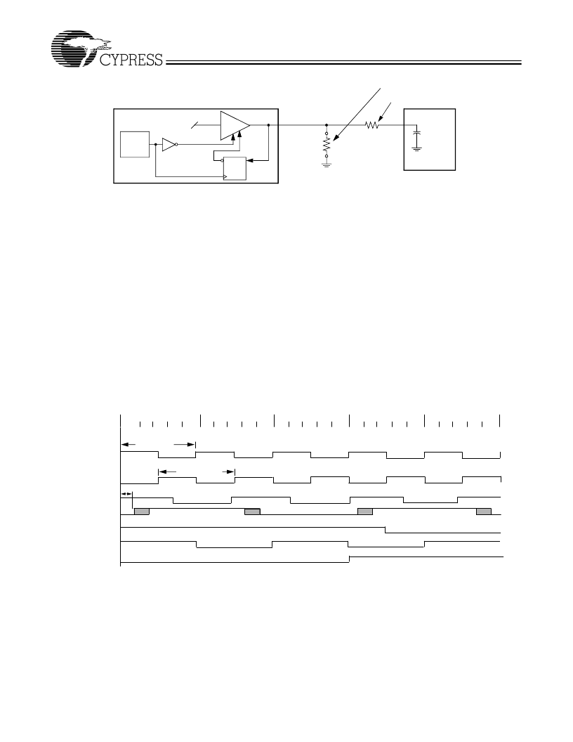
Power Down Control
W229B provides one PWRDWN# signal to place the device in
low-power mode. In low-power mode, the PLLs are turned off
and all clock outputs are driven LOW.
Power-on
Reset
Timer
Output Three-state
Data
Latch
Hold
Output
Low
Q
D
W229B
Clock Load
Output
10 k
Output Strapping Resistor
Series Termination Resistor
Figure 1. Input Logic Selection Through Resistor Load Option.
CPU 66-MHz
SDRAM 100-MHz
3V66 66-MHz
PCI 33-MHz
REF 14.318-MHz
USB 48-MHz
APIC
0 ns
Figure 2. Group Offset Waveforms (66-MHz CPU Clock, 100-MHz SDRAM Clock).
40 ns
30 ns
20 ns
10 ns
SDRAM 100 Period
CPU 100 Period
Hub-PC
相關(guān)PDF資料 |
PDF描述 |
|---|---|
| W22B64A-15 | x4 SRAM |
| W22B64A-20 | x4 SRAM |
| W22B64A-25 | x4 SRAM |
| W22B64AJ-15 | x4 SRAM |
| W22B64AJ-20 | x4 SRAM |
相關(guān)代理商/技術(shù)參數(shù) |
參數(shù)描述 |
|---|---|
| W229BH | 制造商:Cypress Semiconductor 功能描述:PLL Frequency Generator Dual 56-Pin SSOP 制造商:Rochester Electronics LLC 功能描述:TIMING DEVICE - Bulk |
| W229BHT | 制造商:Cypress Semiconductor 功能描述:PLL Frequency Generator Dual 56-Pin SSOP T/R 制造商:Rochester Electronics LLC 功能描述:TIMING DEVICE - Bulk |
| W229E12 | 制造商:OMRON INDUSTRIAL AUTOMATION 功能描述:C200H-AD002 Op. Manual DX CODE ZA |
| W22B20001-AZZ00-000 | 制造商:Carling Technologies 功能描述:W-SERIES ROCKER SWITCH - Bulk |
| W22B64A-15 | 制造商:未知廠家 制造商全稱(chēng):未知廠家 功能描述:x4 SRAM |
發(fā)布緊急采購(gòu),3分鐘左右您將得到回復(fù)。