- 您現在的位置:買賣IC網 > PDF目錄202134 > W25Q32BVZEAG (WINBOND ELECTRONICS CORP) 32M X 1 SPI BUS SERIAL EEPROM, PDSO8 PDF資料下載
參數資料
| 型號: | W25Q32BVZEAG |
| 廠商: | WINBOND ELECTRONICS CORP |
| 元件分類: | PROM |
| 英文描述: | 32M X 1 SPI BUS SERIAL EEPROM, PDSO8 |
| 封裝: | 8 X 6 MM, GREEN, WSON-8 |
| 文件頁數: | 18/79頁 |
| 文件大?。?/td> | 1090K |
| 代理商: | W25Q32BVZEAG |
第1頁第2頁第3頁第4頁第5頁第6頁第7頁第8頁第9頁第10頁第11頁第12頁第13頁第14頁第15頁第16頁第17頁當前第18頁第19頁第20頁第21頁第22頁第23頁第24頁第25頁第26頁第27頁第28頁第29頁第30頁第31頁第32頁第33頁第34頁第35頁第36頁第37頁第38頁第39頁第40頁第41頁第42頁第43頁第44頁第45頁第46頁第47頁第48頁第49頁第50頁第51頁第52頁第53頁第54頁第55頁第56頁第57頁第58頁第59頁第60頁第61頁第62頁第63頁第64頁第65頁第66頁第67頁第68頁第69頁第70頁第71頁第72頁第73頁第74頁第75頁第76頁第77頁第78頁第79頁
W25Q32BV
Publication Release Date: April 01, 2011
- 25 -
Revision F
(IO
1)
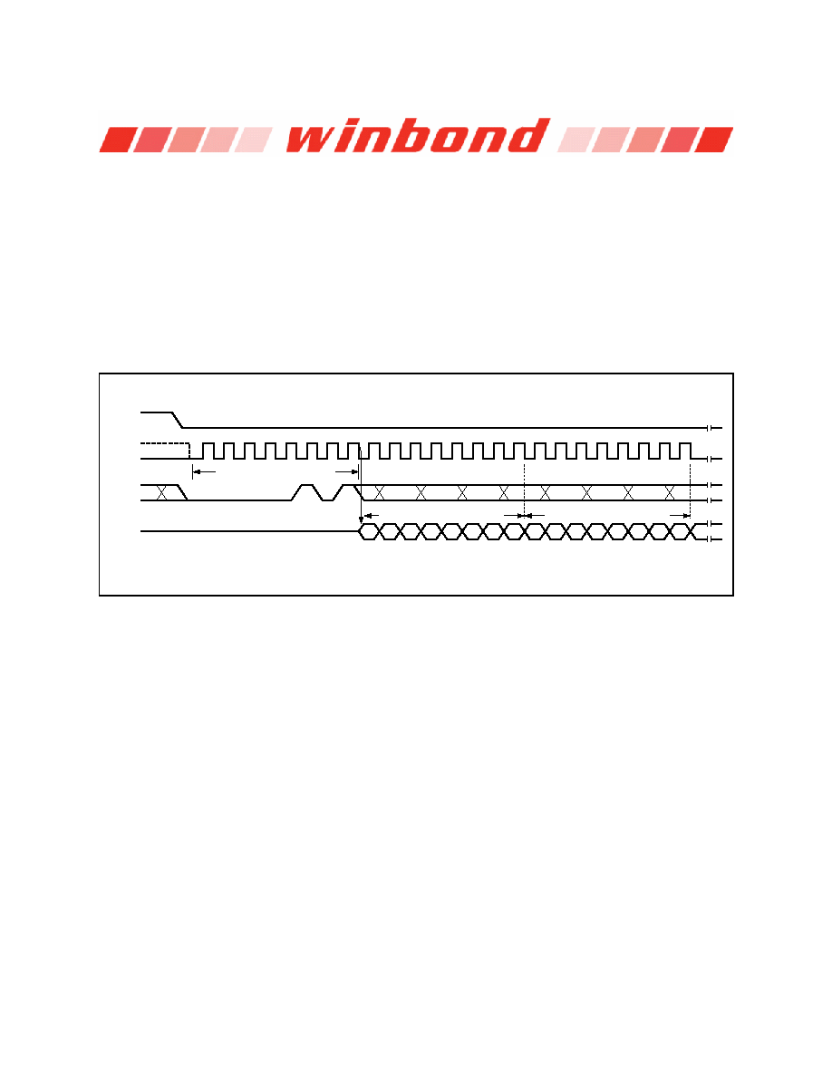
7.2.8 Read Status Register-1 (05h) and Read Status Register-2 (35h)
The Read Status Register instructions allow the 8-bit Status Registers to be read. The instruction is
entered by driving /CS low and shifting the instruction code “05h” for Status Register-1 or “35h” for Status
Register-2 into the DI pin on the rising edge of CLK. The status register bits are then shifted out on the DO
pin at the falling edge of CLK with most significant bit (MSB) first as shown in Figure 7. The Status
Register bits are shown in Figure 3a and 3b and include the BUSY, WEL, BP2-BP0, TB, SEC, SRP0,
SRP1, QE, LB[3:1], CMP and SUS bits (see Status Register section earlier in this datasheet).
The Read Status Register instruction may be used at any time, even while a Program, Erase or Write
Status Register cycle is in progress. This allows the BUSY status bit to be checked to determine when the
cycle is complete and if the device can accept another instruction. The Status Register can be read
continuously, as shown in Figure 7. The instruction is completed by driving /CS high.
/CS
CLK
DI
(IO
0)
DO
Mode 0
Mode 3
0
1
2
3
4
5
6
7
Instruction (05h or 35h)
High Impedance
8
9
10
11
12
13
14
15
16
17
18
19
20
21
22
23
7
6
5
4
3
2
1
0
7
6
5
4
3
2
1
0
7
Status Register 1 or 2 out
**
= MSB
*
Figure 7. Read Status Register Instruction Sequence Diagram
7.2.9 Write Status Register (01h)
The Write Status Register instruction allows the Status Register to be written. Only non-volatile Status
Register bits SRP0, SEC, TB, BP2, BP1, BP0 (bits 7 thru 2 of Status Register-1) and CMP, LB3, LB2,
LB1, QE, SRP1 (bits 14 thru 8 of Status Register-2) can be written to. All other Status Register bit
locations are read-only and will not be affected by the Write Status Register instruction. LB[3:1] are non-
volatile OTP bits, once it is set to 1, it can not be cleared to 0. The Status Register bits are shown in
Figure 3 and described in 7.1.
To write non-volatile Status Register bits, a standard Write Enable (06h) instruction must previously have
been executed for the device to accept the Write Status Register Instruction (Status Register bit WEL
must equal 1). Once write enabled, the instruction is entered by driving /CS low, sending the instruction
code “01h”, and then writing the status register data byte as illustrated in Figure 8.
To write volatile Status Register bits, a Write Enable for Volatile Status Register (50h) instruction must
have been executed prior to the Write Status Register instruction (Status Register bit WEL remains 0).
However, SRP1 and LB3, LB2, LB1 can not be changed from “1” to “0” because of the OTP protection for
these bits. Upon power off, the volatile Status Register bit values will be lost, and the non-volatile Status
Register bit values will be restored when power on again.
相關PDF資料 |
PDF描述 |
|---|---|
| W3EG6466S335AD4M | 64M X 64 DDR DRAM MODULE, 0.7 ns, DMA200 |
| W3EG7264S335AD4SG | 64M X 72 DDR DRAM MODULE, 0.7 ns, DMA200 |
| WF1M32B-120G2UI3A | 1M X 32 FLASH 3.3V PROM MODULE, 120 ns, CQFP68 |
| WF1M32B-120H1I3A | 1M X 32 FLASH 3.3V PROM MODULE, 120 ns, CPGA66 |
| WE128K32N-150G2TC | 128K X 32 EEPROM 5V MODULE, 125 ns, CQFP68 |
相關代理商/技術參數 |
參數描述 |
|---|---|
| W25Q32BVZEAP | 制造商:WINBOND 制造商全稱:Winbond 功能描述:3V 32M-BIT SERIAL FLASH MEMORY WITH DUAL AND QUAD SPI |
| W25Q32BVZEIG | 制造商:Winbond Electronics Corp 功能描述:32MB SPI FLASH |
| W25Q32BVZEIP | 制造商:WINBOND 制造商全稱:Winbond 功能描述:3V 32M-BIT SERIAL FLASH MEMORY WITH DUAL AND QUAD SPI |
| W25Q32BVZPAG | 制造商:WINBOND 制造商全稱:Winbond 功能描述:3V 32M-BIT SERIAL FLASH MEMORY WITH DUAL AND QUAD SPI |
| W25Q32BVZPAP | 制造商:WINBOND 制造商全稱:Winbond 功能描述:3V 32M-BIT SERIAL FLASH MEMORY WITH DUAL AND QUAD SPI |
發(fā)布緊急采購,3分鐘左右您將得到回復。