- 您現(xiàn)在的位置:買賣IC網(wǎng) > PDF目錄245661 > W947D6HBHX5E (WINBOND ELECTRONICS CORP) 8M X 16 DDR DRAM, 5 ns, PBGA60 PDF資料下載
參數(shù)資料
| 型號(hào): | W947D6HBHX5E |
| 廠商: | WINBOND ELECTRONICS CORP |
| 元件分類: | DRAM |
| 英文描述: | 8M X 16 DDR DRAM, 5 ns, PBGA60 |
| 封裝: | 8 X 9 MM, 0.80 MM PITCH, HALOGEN FREE AND LEAD FREE, VFBGA-60 |
| 文件頁(yè)數(shù): | 50/60頁(yè) |
| 文件大小: | 1160K |
| 代理商: | W947D6HBHX5E |
第1頁(yè)第2頁(yè)第3頁(yè)第4頁(yè)第5頁(yè)第6頁(yè)第7頁(yè)第8頁(yè)第9頁(yè)第10頁(yè)第11頁(yè)第12頁(yè)第13頁(yè)第14頁(yè)第15頁(yè)第16頁(yè)第17頁(yè)第18頁(yè)第19頁(yè)第20頁(yè)第21頁(yè)第22頁(yè)第23頁(yè)第24頁(yè)第25頁(yè)第26頁(yè)第27頁(yè)第28頁(yè)第29頁(yè)第30頁(yè)第31頁(yè)第32頁(yè)第33頁(yè)第34頁(yè)第35頁(yè)第36頁(yè)第37頁(yè)第38頁(yè)第39頁(yè)第40頁(yè)第41頁(yè)第42頁(yè)第43頁(yè)第44頁(yè)第45頁(yè)第46頁(yè)第47頁(yè)第48頁(yè)第49頁(yè)當(dāng)前第50頁(yè)第51頁(yè)第52頁(yè)第53頁(yè)第54頁(yè)第55頁(yè)第56頁(yè)第57頁(yè)第58頁(yè)第59頁(yè)第60頁(yè)
W947D6HB / W947D2HB
128Mb Mobile LPDDR
Publication Release Date:Jun,17, 2011
- 54 -
Revision A01-003
19. tHZ and tLZ transitions occur in the same access time windows as valid data transitions. These parameters
are not referred to a specific voltage level, but specify when the device is no longer driving (HZ), or begins
driving (LZ).
20. tDQSQ consists of data pin skew and output pattern effects,
and p-channel to n-channel variation of the
output drivers for any given cycle.
21. The specific requirement is that DQS be valid (HIGH, LOW, or some point on a valid transition) on or before
the corresponding CK edge. A valid transition is defined as monotonic and meeting the input slew rate
specifications of the device. When no writes were previously in progress on the bus, DQS will be transitioning
from Hi-Z to logic LOW. If a previous write was in progress, DQS could be HIGH, LOW, or transitioning from
HIGH to LOW at this time, depending on tDQSS.
22. The maximum limit for this parameter is not a device limit. The device operates with a greater value for this
parameter, but system performance (bus turnaround) will degrade accordingly.
23. A low level on DQS may be maintained during High-Z states (DQS drivers disabled) by adding a weak pull-
down element in the system. It is recommended to turn off the weak pull-down element during read and write
bursts (DQS drivers enabled).
24. At least one clock cycle is required during tWR time when in auto precharge mode.
25. tDAL = (tWR/tCK) + (tRP/tCK): for each of the terms, if not already an integer,
round to the next higher
integer.
26. There must be at least two clock pulses during the tXSR period.
27. There must be at least one clock pulse during the tXP period.
28. A maximum of 8 Refresh commands can be posted to any given LPDDR SDRAM, meaning that the maximum
absolute interval between any Refresh command and the next Refresh command is 8*tREFI.
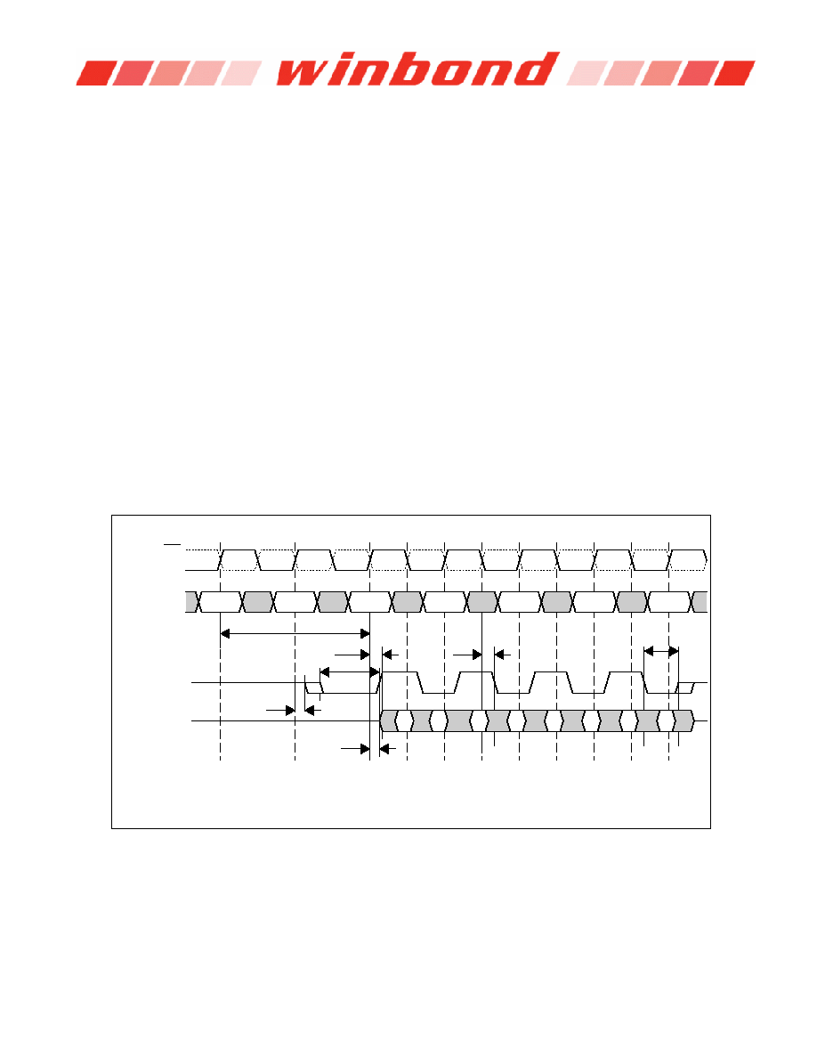
8.5.1 CAS Latency Definition (With CL=3)
CL=3
tLZmin
tRPRE
tDQSCKmin
tRPST
T5n
T5
T4n
T3n
T2n
T4
T3
T2
READ
NOP
Command
CK
DQS
All DQ,
collectively
1)DQ transitioning after DQS transition define tDQSQ window.
2)ALL DQ must transition by tDQSQ after DQS transitions, regardless of tAC
3)tAC is the DQ output window relative to CK,and is the long term component of DQ skew.
T0
T1
T2
T2n
T3
T3n
T4
T4n
T5
T5n
T6
tLZmin
相關(guān)PDF資料 |
PDF描述 |
|---|---|
| WS57C256F-70LMB | 32K X 8 UVPROM, 70 ns, CQCC32 |
| WMS128K8C-120FEIEA | 128K X 8 STANDARD SRAM, 120 ns, CDFP32 |
| WMS128K8L-100FEIE | 128K X 8 STANDARD SRAM, 100 ns, CDFP32 |
| WMS128K8L-120FECEA | 128K X 8 STANDARD SRAM, 120 ns, CDFP32 |
| WMS128K8L-120DRIEA | 128K X 8 STANDARD SRAM, 120 ns, CDSO32 |
相關(guān)代理商/技術(shù)參數(shù) |
參數(shù)描述 |
|---|---|
| W947D6HBHX5I | 制造商:WINBOND 制造商全稱:Winbond 功能描述:128Mb Mobile LPDDR |
| W947D6HBHX5I TR | 制造商:Winbond Electronics Corp 功能描述: |
| W947D6HBHX6E | 制造商:Winbond Electronics Corp 功能描述:IC LPDDR SDRAM 128MBIT 60VFBGA |
| W947D6HBHX6G | 制造商:WINBOND 制造商全稱:Winbond 功能描述:128Mb Mobile LPDDR |
| W948D2FB | 制造商:WINBOND 制造商全稱:Winbond 功能描述:256Mb Mobile LPDDR |
發(fā)布緊急采購(gòu),3分鐘左右您將得到回復(fù)。