- 您現(xiàn)在的位置:買賣IC網(wǎng) > PDF目錄140416 > WED9LC6816V1312BC (WHITE ELECTRONIC DESIGNS CORP) SPECIALTY MEMORY CIRCUIT, PBGA153 PDF資料下載
參數(shù)資料
| 型號(hào): | WED9LC6816V1312BC |
| 廠商: | WHITE ELECTRONIC DESIGNS CORP |
| 元件分類: | 存儲(chǔ)器 |
| 英文描述: | SPECIALTY MEMORY CIRCUIT, PBGA153 |
| 封裝: | 14 X 22 MM, MO-163, BGA-153 |
| 文件頁(yè)數(shù): | 21/26頁(yè) |
| 文件大小: | 324K |
| 代理商: | WED9LC6816V1312BC |
第1頁(yè)第2頁(yè)第3頁(yè)第4頁(yè)第5頁(yè)第6頁(yè)第7頁(yè)第8頁(yè)第9頁(yè)第10頁(yè)第11頁(yè)第12頁(yè)第13頁(yè)第14頁(yè)第15頁(yè)第16頁(yè)第17頁(yè)第18頁(yè)第19頁(yè)第20頁(yè)當(dāng)前第21頁(yè)第22頁(yè)第23頁(yè)第24頁(yè)第25頁(yè)第26頁(yè)
WED9LC6816V
4
White Electronic Designs Corporation (602) 437-1520 www.whiteedc.com
White Electronic Designs
September, 2003
Rev. 1
White Electronic Designs Corp. reserves the right to change products or specications without notice.
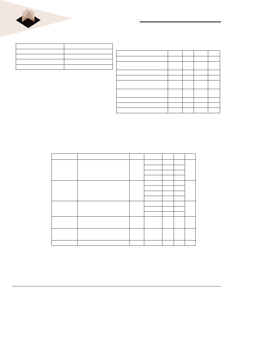
Absolute Maximum Ratings
*Stress greater than those listed under "Absolute Maximum Ratings" may cause
permanent damage to the device. This is a stress rating only and functional
operation of the device at these or any other conditions greater than those indicated
in operational sections of this specications is not implied. Exposure to absolute
maximum rating conditions for extended periods may affect reliability.
(VCC = 3.3V -5% / +10% unless otherwise noted; 0°C tA 70°C,
Commercial; -40°C tA 85°C, Industrial)
NOTES:
1.
All voltages referenced to VSS (GND).
2.
Overshoot: VIH +6.0V for t tKC/2
Underershoot: VIL -2.0V for t tKC/2
(VCC = 3.3V -5% / +10% unless otherwise noted; 0°C tA 70°C, Commercial; -40°C tA 85°C, Industrial)
NOTES:
1.
ICC (operating) is specied with no output current. ICC (operating) increases with faster cycle times and greater output loading.
2.
"Device idle" means device is deselected (CE = VIH) Clock is running at max frequency and Addresses are switching each cycle.
3.
Typical values are measured at 3.3V, 25°C. ICC (operating) is specied at specied frequency.
Voltage on VCC Relative to VSS
-0.5V to +4.6V
VIN (DQx)
-0.5V to VCC +0.5V
Storage Temperature (BGA)
-55°C to +125°C
Junction Temperature
+150°C
Short Circuit Output Current
100 mA
Recommended DC Operating Conditions
Parameter
Symbol
Min
Max
Units
Supply Voltage (1)
VCC
3.135
3.6
V
Input High Voltage (1,2)
VIH
2.0
VCC
+0.3
V
Input Low Voltage (1,2)
VIL
-0.3
0.8
V
Input Leakage Current 0 VIN VCC
ILI
-10
10
μA
Output Leakage (Output Disabled)
0 VIN VCC
ILO
-10
10
μA
SSRAM Output High (IOH = -4mA)
(1)
VOH
2.4
—
V
SSRAM Output Low (IOL = 8mA) (1)
VOL
—
0.4
V
SDRAM Output High (IOH = -2mA)
VOH
2.4
—
V
SDRAM Output Low (IOL = 2mA)
VOL
—
0.4
V
DC ELECTRICAL CHARACTERISTICS
Description
Conditions
Symbol Frequency
Typ
Max
Units
Power Supply
Current
Operating (1,2,3)
SSRAM Active / DRAM Auto Refresh
ICC1
133MHz
500
625
mA
150MHz
500
650
166MHz
550
700
200MHz
600
800
Power Supply
Current
Operating (1,2,3)
SSRAM Active / DRAM Idle
ICC2
133MHz
325
425
mA
150MHz
350
450
166MHz
400
495
200MHz
450
585
Power Supply
Current
Operating (1,2,3)
SSRAM Active / SSRAM Idle
ICC3
83MHz
500
625
mA
100MHz
500
650
125MHz
550
700
CMOS Standby
SSCE# and SDCE# VCC -0.2V, All
other inputs at VSS +0.2 VIN or VIN
VCC -0.2V, CK frequency = 0
ISB1
20.0
40.0
mA
TTL Standby
SSCE# and SDCE# VIH min All
other inputs at VIL max VIN or VIN
VCC -0.2V, CK frequency = 0
ISB2
30.0
55.0
mA
Auto Refresh
ICC5
250
300
mA
相關(guān)PDF資料 |
PDF描述 |
|---|---|
| W3EG2256M72ASSR202JD3SG | 512M X 72 DDR DRAM MODULE, 0.8 ns, DMA184 |
| W3EG2256M72ASSR263AJD3SG | 512M X 72 DDR DRAM MODULE, 0.75 ns, DMA184 |
| W3DG6463V10D2-S | 64M X 64 SYNCHRONOUS DRAM MODULE, 6 ns, DMA168 |
| WF128K32-150G4I | 512K X 8 FLASH 12V PROM MODULE, 150 ns, CQFP68 |
| WF2M32-80G4TC | 8M X 8 FLASH 12V PROM MODULE, 80 ns, CQFP68 |
相關(guān)代理商/技術(shù)參數(shù) |
參數(shù)描述 |
|---|---|
| WED9LC6816V1312BI | 制造商:未知廠家 制造商全稱:未知廠家 功能描述:256K X 32 SSRAM/ 4M X 32 SDRAM |
| WED9LC6816V1510BC | 制造商:未知廠家 制造商全稱:未知廠家 功能描述:256K X 32 SSRAM/ 4M X 32 SDRAM |
| WED9LC6816V1510BI | 制造商:未知廠家 制造商全稱:未知廠家 功能描述:256K X 32 SSRAM/ 4M X 32 SDRAM |
| WED9LC6816V1512BC | 制造商:未知廠家 制造商全稱:未知廠家 功能描述:256K X 32 SSRAM/ 4M X 32 SDRAM |
| WED9LC6816V1512BI | 制造商:未知廠家 制造商全稱:未知廠家 功能描述:256K X 32 SSRAM/ 4M X 32 SDRAM |
發(fā)布緊急采購(gòu),3分鐘左右您將得到回復(fù)。