- 您現(xiàn)在的位置:買賣IC網(wǎng) > PDF目錄362132 > ADCRM Analog-to-Digital Reference Manual PDF資料下載
參數(shù)資料
| 型號: | ADCRM |
| 英文描述: | Analog-to-Digital Reference Manual |
| 中文描述: | 模擬到數(shù)字參考手冊 |
| 文件頁數(shù): | 33/46頁 |
| 文件大小: | 415K |
| 代理商: | ADCRM |
第1頁第2頁第3頁第4頁第5頁第6頁第7頁第8頁第9頁第10頁第11頁第12頁第13頁第14頁第15頁第16頁第17頁第18頁第19頁第20頁第21頁第22頁第23頁第24頁第25頁第26頁第27頁第28頁第29頁第30頁第31頁第32頁當前第33頁第34頁第35頁第36頁第37頁第38頁第39頁第40頁第41頁第42頁第43頁第44頁第45頁第46頁
ADC
REFERENCE MANUAL
PIN CONNECTION CONSIDERATIONS
For More Information On This Product,
Go to: www.freescale.com
MOTOROLA
6-3
cal range of capacitors that still have good high frequency characteristics). This capac-
itor has two effects. First, it helps attenuate any noise that may exist on the input.
Second, it sources charge during the sample period when the analog signal source is
a high-impedance source.
Series resistance can be used with the capacitor on an input pin to implement a simple
RC filter. The maximum level of filtering at the input pins is application dependent and
is based on the bandpass characteristics required to accurately track the dynamic
characteristics of an input. Simple RC filtering at the pin may be limited by the source
(Refer to
6.3.2 Error Resulting from Leakage
.) In some cases, the size of the capac-
itor at the pin may be very small.
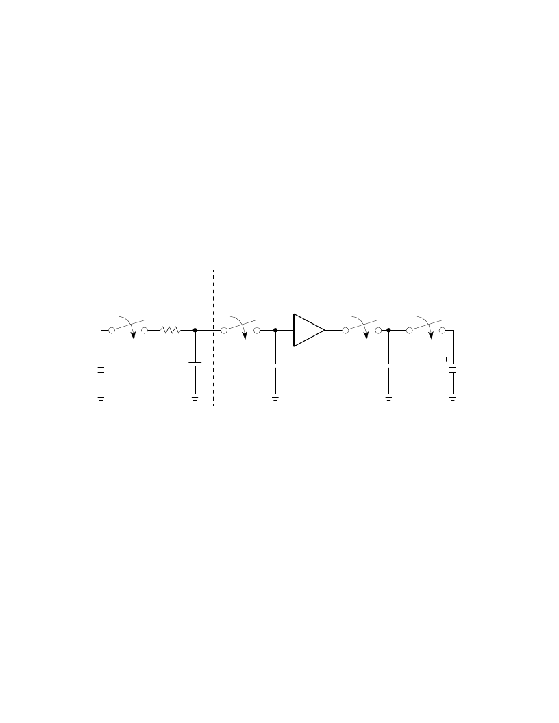
Figure 6-3
is a simplified model of an input channel. Refer to this model in the follow-
ing discussion of the interaction between the user's external circuitry and the circuitry
inside the ADC.
Figure 6-3 Electrical Model of an A/D Input Pin
In
Figure 6-3
, R
F
and C
F
comprise the user's external filter circuit. C
S
is the internal
sample capacitor. The value for this capacitor is 2 pF. Each channel has its own ca-
pacitor. The 2-pF capacitor is never precharged: it retains the value of the last sample.
V
I
is an internal voltage source used to precharge the DAC capacitor array (C
DAC
) be-
fore each sample. The value of this supply is V
DD
/2, or 2.5 volts for 5-volt operation.
The following paragraphs provide a simplified description of the interaction between
the ADC and the user's external circuitry. This circuitry is assumed to be a simple RC
low-pass filter passing a signal from a source to the ADC input pin. The following sim-
plifying assumptions are made:
S1
S2
AMP
R
F
S4
S3
C
DAC
V
I
C
S
C
F
V
SRC
INTERNAL CIRCUIT MODEL
EXTERNAL CIRCUIT
= Source voltage
V
SRC
R
F
C
F
C
S
C
DAC
V
I
= Internal voltage source for precharge (V
DD
/2)
= Internal capacitance (for a bypassed channel, this is the C
DAC
capacitance)
= DAC capacitor array
= Filter impedance (source impedance included)
= Filter capacitor
F
Freescale Semiconductor, Inc.
n
.
相關PDF資料 |
PDF描述 |
|---|---|
| ADCS-1021 | ECONOLINE: REC3-S_DRW(Z)/H* - 3W DIP Package- 1kVDC Isolation- Wide Input 2:1 & 4:1- Regulated Output- 100% Burned In- UL94V-0 Package Material- Continuous Short Circiut Protection- Efficiency to 80% |
| ADCS-2021 | CMOS Image Sensors |
| ADCS-1121 | Monochrome CMOS Image Sensor (CIF) |
| ADCS-2121 | Monochrome CMOS Image Sensor (VGA) |
| ADC | |
相關代理商/技術參數(shù) |
參數(shù)描述 |
|---|---|
| ADCS-1021 | 制造商:AGILENT 制造商全稱:AGILENT 功能描述:CMOS Image Sensors |
| ADCS-1120 | 制造商:AGILENT 制造商全稱:AGILENT 功能描述:Agilent CMOS Monochrome Image Sensors |
| ADCS-1121 | 制造商:未知廠家 制造商全稱:未知廠家 功能描述:Monochrome CMOS Image Sensor (CIF) |
| ADCS-2021 | 制造商:AGILENT 制造商全稱:AGILENT 功能描述:CMOS Image Sensors |
| ADCS-2120 | 制造商:AGILENT 制造商全稱:AGILENT 功能描述:Agilent CMOS Monochrome Image Sensors |
發(fā)布緊急采購,3分鐘左右您將得到回復。