- 您現(xiàn)在的位置:買賣IC網(wǎng) > PDF目錄362132 > ADCRM Analog-to-Digital Reference Manual PDF資料下載
參數(shù)資料
| 型號: | ADCRM |
| 英文描述: | Analog-to-Digital Reference Manual |
| 中文描述: | 模擬到數(shù)字參考手冊 |
| 文件頁數(shù): | 34/46頁 |
| 文件大小: | 415K |
| 代理商: | ADCRM |
第1頁第2頁第3頁第4頁第5頁第6頁第7頁第8頁第9頁第10頁第11頁第12頁第13頁第14頁第15頁第16頁第17頁第18頁第19頁第20頁第21頁第22頁第23頁第24頁第25頁第26頁第27頁第28頁第29頁第30頁第31頁第32頁第33頁當(dāng)前第34頁第35頁第36頁第37頁第38頁第39頁第40頁第41頁第42頁第43頁第44頁第45頁第46頁
MOTOROLA
6-4
PIN CONNECTION CONSIDERATIONS
For More Information On This Product,
Go to: www.freescale.com
ADC
REFERENCE MANUAL
The source impedance is included with the series resistor of the RC filter.
The external capacitor is perfect (no leakage, no significant dielectric absorption
characteristics, etc.)
All parasitic capacitance associated with the input pin is included in the value of
the external capacitor.
Inductance is ignored.
The “on” resistance of the internal switches is zero ohms and the “off” resistance
is infinite.
6.3.1 Settling Time for the External Circuit
The values for R
F
and C
F
in the user's external circuitry determine the length of time
required to charge C
F
to the source voltage level (V
SRC
). At time t = 0, S1 in
Figure
6-3
closes. S2 is open, disconnecting the internal circuitry from the external circuitry.
Assume that the initial voltage across C
F
is 0. As C
F
charges, the voltage across it is
determined by the following equation, where t is the total charge time:
V
CF
= V
SRC
(1–e
–t/R
F
C
F)
When t = 0, the voltage across C
F
= 0. As t approaches infinity, V
CF
will equal V
SRC
.
(This assumes no internal leakage.) With 10-bit resolution, 1/2 of a count is equal to
1/2048 full-scale value. Assuming worst case (V
SRC
= full scale),
Table 6-1
shows the
required time for C
F
to charge to within 1/2 of a count of the actual source voltage dur-
ing 10-bit conversions. Note that these times are completely independent of the A/D
converter architecture (assuming the ADC is not affecting the charging).
The external circuit described in
Table 6-1
is a low-pass filter. A user interested in
measuring an AC component of the external signal must take the characteristics of this
filter into account.
6.3.2 Error Resulting from Leakage
A series resistor can limit the current to a pin, but input leakage acting through a large
source impedance can degrade A/D accuracy. The maximum input leakage current is
specified in
APPENDIX A ELECTRICAL CHARACTERISTICS
. Input leakage is
greatest at high operating temperatures and as a general rule decreased by one half
for each 10
°
C decrease in temperature.
When V
RH
– V
RL
= 5.12 V, 1 count (assuming 10-bit resolution) corresponds to 5 mV
of input voltage. A typical input leakage of 50 nA acting through 100 k
of external se-
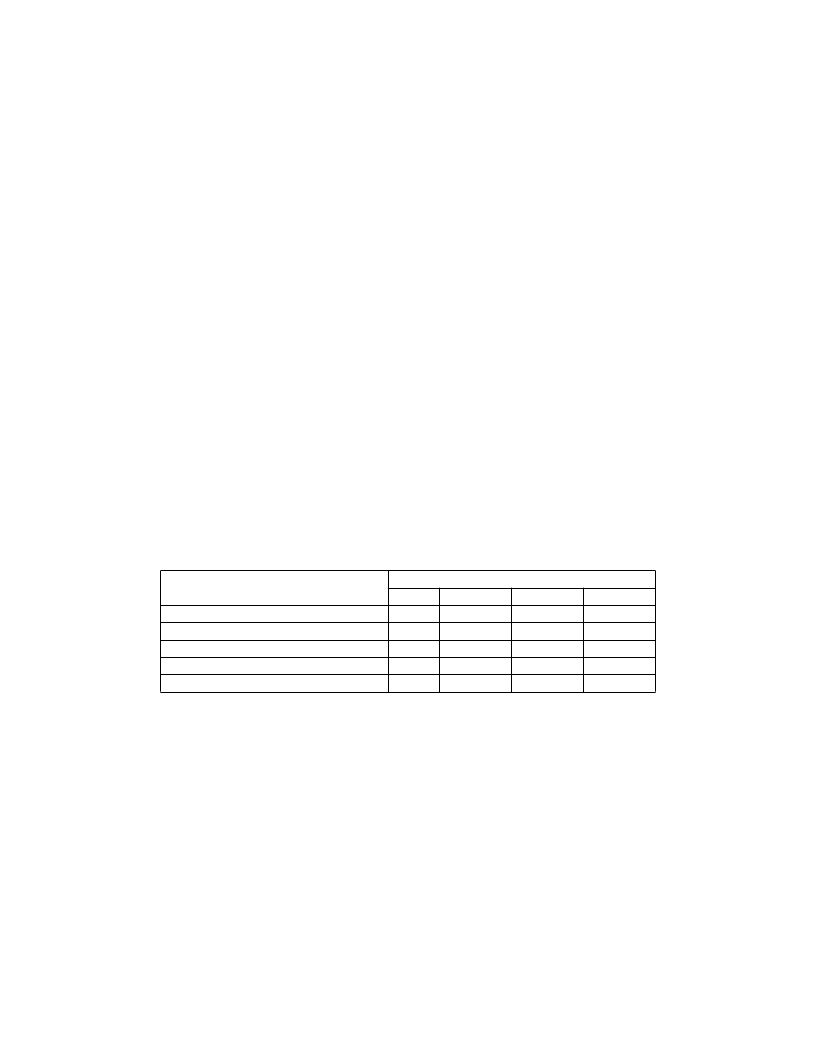
Table 6-1 External Circuit Settling Time (10-Bit Conversions)
Filter
Capacitor
1
μ
F
.1
μ
F
.01
μ
F
.001
μ
F
100 pF
Source Resistance
1 k
7.6 ms
760
μ
s
76
μ
s
7.6
μ
s
760 ns
100
760
μ
s
76
μ
s
7.6
μ
s
760 ns
76 ns
10 k
76 ms
7.6 ms
760
μ
s
76
μ
s
7.6
μ
s
100 k
760 ms
76 ms
7.6 ms
760
μ
s
76
μ
s
F
Freescale Semiconductor, Inc.
n
.
相關(guān)PDF資料 |
PDF描述 |
|---|---|
| ADCS-1021 | ECONOLINE: REC3-S_DRW(Z)/H* - 3W DIP Package- 1kVDC Isolation- Wide Input 2:1 & 4:1- Regulated Output- 100% Burned In- UL94V-0 Package Material- Continuous Short Circiut Protection- Efficiency to 80% |
| ADCS-2021 | CMOS Image Sensors |
| ADCS-1121 | Monochrome CMOS Image Sensor (CIF) |
| ADCS-2121 | Monochrome CMOS Image Sensor (VGA) |
| ADC | |
相關(guān)代理商/技術(shù)參數(shù) |
參數(shù)描述 |
|---|---|
| ADCS-1021 | 制造商:AGILENT 制造商全稱:AGILENT 功能描述:CMOS Image Sensors |
| ADCS-1120 | 制造商:AGILENT 制造商全稱:AGILENT 功能描述:Agilent CMOS Monochrome Image Sensors |
| ADCS-1121 | 制造商:未知廠家 制造商全稱:未知廠家 功能描述:Monochrome CMOS Image Sensor (CIF) |
| ADCS-2021 | 制造商:AGILENT 制造商全稱:AGILENT 功能描述:CMOS Image Sensors |
| ADCS-2120 | 制造商:AGILENT 制造商全稱:AGILENT 功能描述:Agilent CMOS Monochrome Image Sensors |
發(fā)布緊急采購,3分鐘左右您將得到回復(fù)。