- 您現(xiàn)在的位置:買賣IC網(wǎng) > PDF目錄378286 > ADV7183ABST (ANALOG DEVICES INC) Multiformat SDTV Video Decoder PDF資料下載
參數(shù)資料
| 型號: | ADV7183ABST |
| 廠商: | ANALOG DEVICES INC |
| 元件分類: | 顏色信號轉(zhuǎn)換 |
| 英文描述: | Multiformat SDTV Video Decoder |
| 中文描述: | COLOR SIGNAL DECODER, PQFP80 |
| 封裝: | LEAD FREE, MS-026-BEC, LQFP-80 |
| 文件頁數(shù): | 53/104頁 |
| 文件大?。?/td> | 894K |
| 代理商: | ADV7183ABST |
第1頁第2頁第3頁第4頁第5頁第6頁第7頁第8頁第9頁第10頁第11頁第12頁第13頁第14頁第15頁第16頁第17頁第18頁第19頁第20頁第21頁第22頁第23頁第24頁第25頁第26頁第27頁第28頁第29頁第30頁第31頁第32頁第33頁第34頁第35頁第36頁第37頁第38頁第39頁第40頁第41頁第42頁第43頁第44頁第45頁第46頁第47頁第48頁第49頁第50頁第51頁第52頁當前第53頁第54頁第55頁第56頁第57頁第58頁第59頁第60頁第61頁第62頁第63頁第64頁第65頁第66頁第67頁第68頁第69頁第70頁第71頁第72頁第73頁第74頁第75頁第76頁第77頁第78頁第79頁第80頁第81頁第82頁第83頁第84頁第85頁第86頁第87頁第88頁第89頁第90頁第91頁第92頁第93頁第94頁第95頁第96頁第97頁第98頁第99頁第100頁第101頁第102頁第103頁第104頁
ADV7183A
CRC_ENABLE CRC CGMS-A Sequence (SDP),
Address 0xB2, [2]
For certain video sources, the CRC data bits may have an
invalid format. In such circumstances, the CRC checksum
validation procedure can be disabled. The CGMSD bit goes
high if the rising edge of the start bit is detected within a time
window.
Table 142. CRC_ENABLE Function
CRC_ENABLE
Description
0
No CRC check performed. The CGMSD bit goes
high if the rising edge of the start bit is detected
within a time window.
1*
Use CRC checksum to validate the CGMS-A
sequence. The CGMSD bit goes high for a valid
checksum. ADI recommended setting.
*Default value.
Rev. A | Page 53 of 104
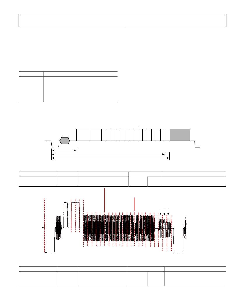
Wide Screen Signaling Data
WSS1[7:0] (SDP), Address 0x91, [7:0], WSS2[7:0] (SDP),
Address 0x92, [7:0]
Figure 31 shows the bit correspondence between the analog
video waveform and the WSS1/WSS2 registers. Please note that
WSS2[7:6] are undetermined and should be masked out by
software.
EDTV Data Registers
EDTV1[7:0] (SDP), Address 0x93, [7:0], EDTV2[7:0] (SDP),
Address 0x94, [7:0], EDTV3[7:0] (SDP), Address 0x95, [7:0]
Figure 32 shows the bit correspondence between the analog
video waveform and the EDTV1/EDTV2/EDTV3 registers.
Note that EDTV3[7:6] are undetermined and should be masked
out by software. EDTV3[5] is reserved for future use and, for
now, will contain 0. The three LSBs of the EDTV waveform are
currently not supported.
0
ACTIVE
VIDEO
WSS2[5:0]
WSS1[7:0]
SRUN-IN
START
CODE
0
1
2
3
4
5
6
7
0
1
2
3
4
5
11.0
μ
s
38.4
μ
s
42.5
μ
s
Figure 31. SDP WSS Data Extraction
Table 143. SDP WSS Access Information
Signal Name
WSS1 [7:0]
WSS2 [5:0]
Block
SDP
SDP
Register Location
WSS 1 [7:0]
WSS 2 [5:0]
Address
Register Default Value
Readback Only
Readback Only
145d
146d
91h
92h
EDTV1[7:0]
EDTV2[7:0]
EDTV3[5:0]
NOT SUPPORTED
0
1
3
4
5
6
7
0
1
2
3 4
5
6
7
0
1
2
3
4
5
2
0
Figure 32. SDP EDTV Data Extraction
Table 144. SDP EDTV Access Information
Signal Name
EDTV1[7:0]
EDTV2[7:0]
EDTV3[7:0]
Block
SDP
SDP
SDP
Register Location
EDTV 1 [7:0]
EDTV 2 [7:0]
EDTV 3 [7:0]
Address
Register Default Value
Readback Only
Readback Only
Readback Only
147d
148d
149d
93h
94h
95h
相關(guān)PDF資料 |
PDF描述 |
|---|---|
| ADV7183AKST | Multiformat SDTV Video Decoder |
| ADV7330 | Multiformat 11-Bit Triple DAC Video Encoder |
| ADV7330KST | Multiformat 11-Bit Triple DAC Video Encoder |
| ADXL321 | Small and Thin 18 g Accelerometer |
| ADXL321EB | Small and Thin 18 g Accelerometer |
相關(guān)代理商/技術(shù)參數(shù) |
參數(shù)描述 |
|---|---|
| ADV7183AKST | 制造商:Analog Devices 功能描述:MULTIFORMAT SDTV VIDEO DECODER 制造商:Rochester Electronics LLC 功能描述:10BIT NTSC/PAL/SECAMVIDDECOD I.C - Tape and Reel 制造商:Analog Devices 功能描述:IC VIDEO ENCODER |
| ADV7183AKST-U1 | 制造商:Analog Devices 功能描述:VID DECODER 80LQFP - Bulk |
| ADV7183AKST-X2 | 制造商:Analog Devices 功能描述:VID DECODER - Bulk |
| ADV7183AXST | 制造商:Analog Devices 功能描述:VIDEO DECODER I.C. - Bulk |
| ADV7183AXST-X2 | 制造商:Analog Devices 功能描述:VIDEO DECODER I.C. - Bulk |
發(fā)布緊急采購,3分鐘左右您將得到回復。