- 您現(xiàn)在的位置:買賣IC網(wǎng) > PDF目錄366891 > CR16HCT5 PDF資料下載
參數(shù)資料
| 型號: | CR16HCT5 |
| 文件頁數(shù): | 139/157頁 |
| 文件大小: | 1256K |
| 代理商: | CR16HCT5 |
第1頁第2頁第3頁第4頁第5頁第6頁第7頁第8頁第9頁第10頁第11頁第12頁第13頁第14頁第15頁第16頁第17頁第18頁第19頁第20頁第21頁第22頁第23頁第24頁第25頁第26頁第27頁第28頁第29頁第30頁第31頁第32頁第33頁第34頁第35頁第36頁第37頁第38頁第39頁第40頁第41頁第42頁第43頁第44頁第45頁第46頁第47頁第48頁第49頁第50頁第51頁第52頁第53頁第54頁第55頁第56頁第57頁第58頁第59頁第60頁第61頁第62頁第63頁第64頁第65頁第66頁第67頁第68頁第69頁第70頁第71頁第72頁第73頁第74頁第75頁第76頁第77頁第78頁第79頁第80頁第81頁第82頁第83頁第84頁第85頁第86頁第87頁第88頁第89頁第90頁第91頁第92頁第93頁第94頁第95頁第96頁第97頁第98頁第99頁第100頁第101頁第102頁第103頁第104頁第105頁第106頁第107頁第108頁第109頁第110頁第111頁第112頁第113頁第114頁第115頁第116頁第117頁第118頁第119頁第120頁第121頁第122頁第123頁第124頁第125頁第126頁第127頁第128頁第129頁第130頁第131頁第132頁第133頁第134頁第135頁第136頁第137頁第138頁當前第139頁第140頁第141頁第142頁第143頁第144頁第145頁第146頁第147頁第148頁第149頁第150頁第151頁第152頁第153頁第154頁第155頁第156頁第157頁
139
www.national.com
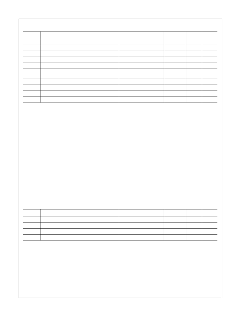
Flash EEPROM Data Programming
Flash EEPROM ISP-Memory Programming
Symbol
Parameter
Conditions
Min
Max
Units
re-programming time
a
Programming pulse width
b
Erase pulse width
c
Charge pump power-up time
d
Program/erase transition time
e
Charge pump enable hold time
a. One re-programming cycle involves one erase pulse followed by programming of four bytes.
1.32
30
4
10
5
1
-
ms
μ
s
ms
μ
s
μ
s
clock
cycles
μ
s
cycles
cycles
years
t
PWD
t
EWD
t
SDD
t
TTD
t
PED
b. The programming pulse width is determined by the following equation:
t
PWD
= T
clk
x (FTDIV+1) x (FTPROG+1), where T
clk
is the system clock period, FTDIV is the contents of the DMPSLR register
and FTPROG is the contents of the DMPROG register.
40
-
-
-
-
c. The erase pulse width is determined by the following equation:
t
EWD
= T
clk
x (FTDIV+1) x 4 x (FTER+1), where T
clk
is the system clock period, FTDIV is the contents of the DMPSLR register
and FTER is the contents of the DMERASE register.
d. The program/erase start delay time is determined by the following equation:
t
SDD
= T
clk
x (FTDIV+1) x (FTSTART+1), where T
clk
is the system clock period, FTDIV is the contents of the DMPSLR register
and FTSTART is the contents of the DMSTART register.
e. The program/erase transition time is determined by the following equation:
t
TTD
= T
clk
x (FTDIV+1) x (FTTRAN+1), where T
clk
is the system clock period, FTDIV is the contents of the DMPSLR register
and FTTRAN is the contents of the DMTRAN register.
t
EDD
Charge pump power hold time
f
Write/erase endurance (high endurance)
Write/erase endurance (low endurance)
Data retention
f. The program/erase end delay time is determined by the following equation:
t
EDD
= T
clk
x (FTDIV+1) x (FTEND+1), where T
clk
is the system clock period, FTDIV is the contents of the DMPSLR register and
FTEND is the contents of the DMEND register.
5
-
-
-
-
100,000
25,000
100
Symbol
Parameter
Conditions
Min
Max
Units
t
PWI
t
EWI
Programming pulse with
a
Erase pulse width
b
Data retention
a. Programming timing is controlled by the flash EEPROM data memory interface
b. Erase timing is controlled by the flash EEPROM data memory interface
30
1
100
-
40
-
-
μ
s
ms
years
cycles
100K
相關PDF資料 |
PDF描述 |
|---|---|
| CR16HCT5VJE7Y | Microcontroller |
| CR16HCT5VJE8Y | Microcontroller |
| CR16HCT5VJE9Y | Microcontroller |
| CR16HCT9 | |
| CR16HCT9VJE7 | Microcontroller |
相關代理商/技術參數(shù) |
參數(shù)描述 |
|---|---|
| CR16HCT5VJE7Y | 制造商:未知廠家 制造商全稱:未知廠家 功能描述:Microcontroller |
| CR16HCT5VJE8Y | 制造商:未知廠家 制造商全稱:未知廠家 功能描述:Microcontroller |
| CR16HCT5VJE9Y | 制造商:未知廠家 制造商全稱:未知廠家 功能描述:Microcontroller |
| CR16HCT5VJEXY | 制造商:NSC 制造商全稱:National Semiconductor 功能描述:CR16MCT9/CR16MCT5/CR16HCT9/CR16HCT5 16-Bit Reprogrammable/ROM Microcontroller |
| CR16HCT9 | 制造商:NSC 制造商全稱:National Semiconductor 功能描述:CR16MCT9/CR16MCT5/CR16HCT9/CR16HCT5 16-Bit Reprogrammable/ROM Microcontroller |
發(fā)布緊急采購,3分鐘左右您將得到回復。