- 您現(xiàn)在的位置:買(mǎi)賣(mài)IC網(wǎng) > PDF目錄4069 > CS80C286-12 (Intersil)IC CPU 16BIT 5V 12.5MHZ 68-PLCC PDF資料下載
參數(shù)資料
| 型號(hào): | CS80C286-12 |
| 廠商: | Intersil |
| 文件頁(yè)數(shù): | 47/60頁(yè) |
| 文件大?。?/td> | 0K |
| 描述: | IC CPU 16BIT 5V 12.5MHZ 68-PLCC |
| 標(biāo)準(zhǔn)包裝: | 126 |
| 處理器類(lèi)型: | 80C286 16-位 |
| 速度: | 12.5MHz |
| 電壓: | 5V |
| 安裝類(lèi)型: | 表面貼裝 |
| 封裝/外殼: | 68-LCC(J 形引線(xiàn)) |
| 供應(yīng)商設(shè)備封裝: | 68-PLCC(24.23x24.23) |
| 包裝: | 管件 |
第1頁(yè)第2頁(yè)第3頁(yè)第4頁(yè)第5頁(yè)第6頁(yè)第7頁(yè)第8頁(yè)第9頁(yè)第10頁(yè)第11頁(yè)第12頁(yè)第13頁(yè)第14頁(yè)第15頁(yè)第16頁(yè)第17頁(yè)第18頁(yè)第19頁(yè)第20頁(yè)第21頁(yè)第22頁(yè)第23頁(yè)第24頁(yè)第25頁(yè)第26頁(yè)第27頁(yè)第28頁(yè)第29頁(yè)第30頁(yè)第31頁(yè)第32頁(yè)第33頁(yè)第34頁(yè)第35頁(yè)第36頁(yè)第37頁(yè)第38頁(yè)第39頁(yè)第40頁(yè)第41頁(yè)第42頁(yè)第43頁(yè)第44頁(yè)第45頁(yè)第46頁(yè)當(dāng)前第47頁(yè)第48頁(yè)第49頁(yè)第50頁(yè)第51頁(yè)第52頁(yè)第53頁(yè)第54頁(yè)第55頁(yè)第56頁(yè)第57頁(yè)第58頁(yè)第59頁(yè)第60頁(yè)

51
80C286 Instruction Set Summary
Instruction Timing Notes
The instruction clock counts listed below establish the maxi-
mum execution rate of the 80C286. With no delays in bus
cycles, the actual clock count of an 80C286 program will
average 5% more than the calculated clock count, due to
instruction sequences which execute faster than they can be
fetched from memory.
To calculate elapsed times for instruction sequences, multi-
ply the sum of all instruction clock counts, as listed in the
table below, by the processor clock period. An 12.5MHz pro-
cessor clock has a clock period of 80 nanoseconds and
requires an 80C286 system clock (CLK input) of 25MHz.
Instruction Clock Count Assumptions
1. The instruction has been perfected, decoded and is
ready for execution. Control transfer instruction clock
counts include all time required to fetch, decode, and
prepare the next instruction for execution.
2. Bus cycles do not require wait states.
3. There are no processor extension data transfer or local
bus HOLD requests.
4. No exceptions occur during instruction execution.
Instruction Set Summary Notes
Addressing displacements selected by the MOD field are not
shown. If necessary they appear after the instruction fields
shown.
Above/below refers to unsigned value.
Greater refers to more positive signed values.
Less refers to less positive (more negative) signed values
if d = 1, then “to” register; if d = 0 then “from” register
if w = 1, then word instruction; if w = 0, then byte instruction
if s = 0, then 16-bit immediate data form the operand
if s = 1, then an immediate data byte is sign-extended to
form the 16-bit operand
x don’t care
z used for string primitives for comparison with ZF FLAG
If two clock counts are given, the smaller refers to a register
operand and the larger refers to a memory operand
* = add one clock if offset calculation requires summing 3
elements
n = number of times repeated
m = number of bytes of code in next instruction
Level (L) - Lexical nesting level of the procedure
The following comments describe possible exceptions, side
effects and allowed usage for instructions in both operating
modes of the 80C286.
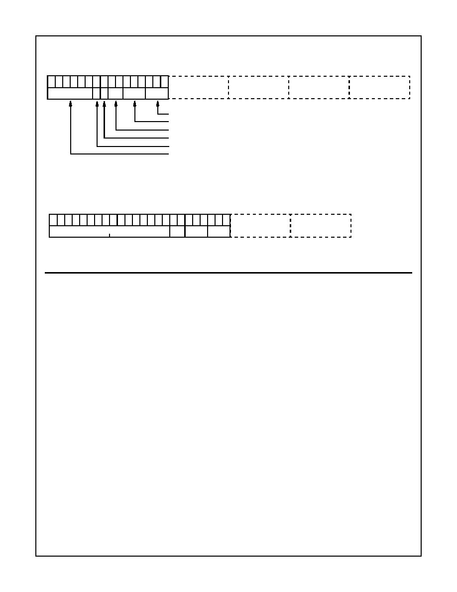
FIGURE 40A. SHORT OPCODE FORMAT EXAMPLE
FIGURE 40B. LONG OPCODE FORMAT EXAMPLE
FIGURE 40. 80C286 INSTRUCTION FORMAT EXAMPLES
Waveforms (Continued)
LOW DISP/DATA
HIGH DISP/DATA
LOW DATA
HIGH DATA
OPCODE
MOD
REG
R/M
dw
BYTE 1
BYTE 2
BYTE 3
BYTE 4
BYTE 5
BYTE 6
765 43210 7654 3210
REGISTER OPERAND REGISTERS TO USE IN OFFSET CALCULATION
REGISTER OPERAND/EXTENSION OF OPCODE
REGISTER MODE/MEMORY MODE WITH DISPLACEMENT LENGTH
WORD/BYTE OPERATION
DIRECTION IS TO REGISTER DIRECTION IS FROM REGISTER
OPERATION (INSTRUCTION) CODE
LOW DISP
HIGH DISP
BYTE 5
BYTE 4
BYTE 3
BYTE 2
BYTE 1
LONG OPCODE
MOD
REG
R/M
7654321 07654321 07654321 0
80C286
相關(guān)PDF資料 |
PDF描述 |
|---|---|
| IP80C88 | IC CPU 8/16BIT 5V 5MHZ 40-DIP |
| SPC5200CBV400B | IC MPU 32BIT 500MHZ 272PBGA |
| ABB85DHBR | CONN EDGECARD 170PS R/A .050 SLD |
| XF2M-2215-1A | CONN FPC 22POS 0.5MM PITCH SMD |
| MPC859TCVR100A | IC MPU POWERQUICC 100MHZ 357PBGA |
相關(guān)代理商/技術(shù)參數(shù) |
參數(shù)描述 |
|---|---|
| CS80C286-1296 | 制造商:Rochester Electronics LLC 功能描述:- Bulk |
| CS80C286-12X136 | 制造商:Rochester Electronics LLC 功能描述:- Bulk |
| CS80C286-16 | 功能描述:微處理器 - MPU CPU 16BIT 5V CMOS 16 MHZ 68PLCC COM RoHS:否 制造商:Atmel 處理器系列:SAMA5D31 核心:ARM Cortex A5 數(shù)據(jù)總線(xiàn)寬度:32 bit 最大時(shí)鐘頻率:536 MHz 程序存儲(chǔ)器大小:32 KB 數(shù)據(jù) RAM 大小:128 KB 接口類(lèi)型:CAN, Ethernet, LIN, SPI,TWI, UART, USB 工作電源電壓:1.8 V to 3.3 V 最大工作溫度:+ 85 C 安裝風(fēng)格:SMD/SMT 封裝 / 箱體:FBGA-324 |
| CS80C286-1696 | 制造商:Rochester Electronics LLC 功能描述:- Bulk |
| CS80C286-2 | 制造商:Harris Corporation 功能描述: |
發(fā)布緊急采購(gòu),3分鐘左右您將得到回復(fù)。