- 您現(xiàn)在的位置:買賣IC網(wǎng) > PDF目錄298976 > CY7C2566KV18-450BZI (CYPRESS SEMICONDUCTOR CORP) 8M X 8 DDR SRAM, 0.37 ns, PBGA165 PDF資料下載
參數(shù)資料
| 型號: | CY7C2566KV18-450BZI |
| 廠商: | CYPRESS SEMICONDUCTOR CORP |
| 元件分類: | SRAM |
| 英文描述: | 8M X 8 DDR SRAM, 0.37 ns, PBGA165 |
| 封裝: | 13 X 15 MM, 1.40 MM HEIGHT, MO-216, FBGA-165 |
| 文件頁數(shù): | 9/28頁 |
| 文件大?。?/td> | 831K |
| 代理商: | CY7C2566KV18-450BZI |
第1頁第2頁第3頁第4頁第5頁第6頁第7頁第8頁當(dāng)前第9頁第10頁第11頁第12頁第13頁第14頁第15頁第16頁第17頁第18頁第19頁第20頁第21頁第22頁第23頁第24頁第25頁第26頁第27頁第28頁
PRELIMINARY
CY7C2566KV18, CY7C2577KV18
CY7C2568KV18, CY7C2570KV18
Document Number: 001-15889 Rev. *D
Page 17 of 28
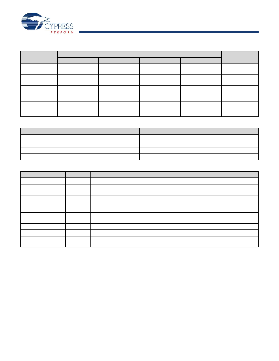
Table 7. Identification Register Definitions
Instruction Field
Value
Description
CY7C2566KV18
CY7C2577KV18
CY7C2568KV18
CY7C2570KV18
Revision Number
(31:29)
000
Version number.
Cypress Device ID
(28:12)
11010111000000100 11010111000001100 11010111000010100 11010111000100100 Defines the type of
SRAM.
Cypress JEDEC ID
(11:1)
00000110100
Allows unique
identification of
SRAM vendor.
ID Register
Presence (0)
1111
Indicates the
presence of an ID
register.
Table 8. Scan Register Sizes
Register Name
Bit Size
Instruction
3
Bypass
1
ID
32
Boundary Scan
109
Table 9. Instruction Codes
Instruction
Code
Description
EXTEST
000
Captures the input and output ring contents.
IDCODE
001
Loads the ID register with the vendor ID code and places the register between TDI and TDO.
This operation does not affect SRAM operation.
SAMPLE Z
010
Captures the input and output contents. Places the boundary scan register between TDI and
TDO. Forces all SRAM output drivers to a High-Z state.
RESERVED
011
Do Not Use: This instruction is reserved for future use.
SAMPLE/PRELOAD
100
Captures the input and output ring contents. Places the boundary scan register between TDI
and TDO. Does not affect the SRAM operation.
RESERVED
101
Do Not Use: This instruction is reserved for future use.
RESERVED
110
Do Not Use: This instruction is reserved for future use.
BYPASS
111
Places the bypass register between TDI and TDO. This operation does not affect SRAM
operation.
相關(guān)PDF資料 |
PDF描述 |
|---|---|
| CY7C293AL-35WC | 2K X 8 UVPROM, 35 ns, CDIP24 |
| CY7C474-15DI | 32K X 9 OTHER FIFO, 15 ns, CDIP28 |
| CY7C474-15PI | 32K X 9 OTHER FIFO, 15 ns, PDIP28 |
| CZ12010T0050GBK | 0 MHz - 3000 MHz 50 ohm RF/MICROWAVE TERMINATION |
| CZ5360D | 25 V, 5 W, SILICON, UNIDIRECTIONAL VOLTAGE REGULATOR DIODE, DO-201AD |
相關(guān)代理商/技術(shù)參數(shù) |
參數(shù)描述 |
|---|---|
| CY7C25682KV18-400BZC | 功能描述:靜態(tài)隨機(jī)存取存儲器 72MB (4Mx18) 1.8v 400MHz DDR II 靜態(tài)隨機(jī)存取存儲器 RoHS:否 制造商:Cypress Semiconductor 存儲容量:16 Mbit 組織:1 M x 16 訪問時間:55 ns 電源電壓-最大:3.6 V 電源電壓-最小:2.2 V 最大工作電流:22 uA 最大工作溫度:+ 85 C 最小工作溫度:- 40 C 安裝風(fēng)格:SMD/SMT 封裝 / 箱體:TSOP-48 封裝:Tray |
| CY7C25682KV18-400BZXC | 功能描述:靜態(tài)隨機(jī)存取存儲器 72MB (4Mx18) 1.8v 400MHz DDR II 靜態(tài)隨機(jī)存取存儲器 RoHS:否 制造商:Cypress Semiconductor 存儲容量:16 Mbit 組織:1 M x 16 訪問時間:55 ns 電源電壓-最大:3.6 V 電源電壓-最小:2.2 V 最大工作電流:22 uA 最大工作溫度:+ 85 C 最小工作溫度:- 40 C 安裝風(fēng)格:SMD/SMT 封裝 / 箱體:TSOP-48 封裝:Tray |
| CY7C25682KV18-450BZC | 功能描述:靜態(tài)隨機(jī)存取存儲器 72MB (4Mx18) 1.8v 450MHz DDR II 靜態(tài)隨機(jī)存取存儲器 RoHS:否 制造商:Cypress Semiconductor 存儲容量:16 Mbit 組織:1 M x 16 訪問時間:55 ns 電源電壓-最大:3.6 V 電源電壓-最小:2.2 V 最大工作電流:22 uA 最大工作溫度:+ 85 C 最小工作溫度:- 40 C 安裝風(fēng)格:SMD/SMT 封裝 / 箱體:TSOP-48 封裝:Tray |
| CY7C25682KV18-500BZC | 功能描述:靜態(tài)隨機(jī)存取存儲器 72MB (4Mx18) 1.8v 500MHz DDR II 靜態(tài)隨機(jī)存取存儲器 RoHS:否 制造商:Cypress Semiconductor 存儲容量:16 Mbit 組織:1 M x 16 訪問時間:55 ns 電源電壓-最大:3.6 V 電源電壓-最小:2.2 V 最大工作電流:22 uA 最大工作溫度:+ 85 C 最小工作溫度:- 40 C 安裝風(fēng)格:SMD/SMT 封裝 / 箱體:TSOP-48 封裝:Tray |
| CY7C25682KV18-550BZXC | 功能描述:靜態(tài)隨機(jī)存取存儲器 72MB (4Mx18) 2.9v 550MHz DDR II 靜態(tài)隨機(jī)存取存儲器 RoHS:否 制造商:Cypress Semiconductor 存儲容量:16 Mbit 組織:1 M x 16 訪問時間:55 ns 電源電壓-最大:3.6 V 電源電壓-最小:2.2 V 最大工作電流:22 uA 最大工作溫度:+ 85 C 最小工作溫度:- 40 C 安裝風(fēng)格:SMD/SMT 封裝 / 箱體:TSOP-48 封裝:Tray |
發(fā)布緊急采購,3分鐘左右您將得到回復(fù)。