- 您現(xiàn)在的位置:買賣IC網(wǎng) > PDF目錄385414 > HY27USxxx (Hynix Semiconductor Inc.) 512Mbit (64Mx8bit / 32Mx16bit) NAND Flash PDF資料下載
參數(shù)資料
| 型號: | HY27USxxx |
| 廠商: | Hynix Semiconductor Inc. |
| 英文描述: | 512Mbit (64Mx8bit / 32Mx16bit) NAND Flash |
| 中文描述: | 512兆(64Mx8bit / 32Mx16bit)NAND閃存 |
| 文件頁數(shù): | 21/43頁 |
| 文件大小: | 729K |
| 代理商: | HY27USXXX |
第1頁第2頁第3頁第4頁第5頁第6頁第7頁第8頁第9頁第10頁第11頁第12頁第13頁第14頁第15頁第16頁第17頁第18頁第19頁第20頁當前第21頁第22頁第23頁第24頁第25頁第26頁第27頁第28頁第29頁第30頁第31頁第32頁第33頁第34頁第35頁第36頁第37頁第38頁第39頁第40頁第41頁第42頁第43頁
Rev 0.6 / Oct. 2004
21
HY27SS(08/16)121M Series
HY27US(08/16)121M Series
512Mbit (64Mx8bit / 32Mx16bit) NAND Flash
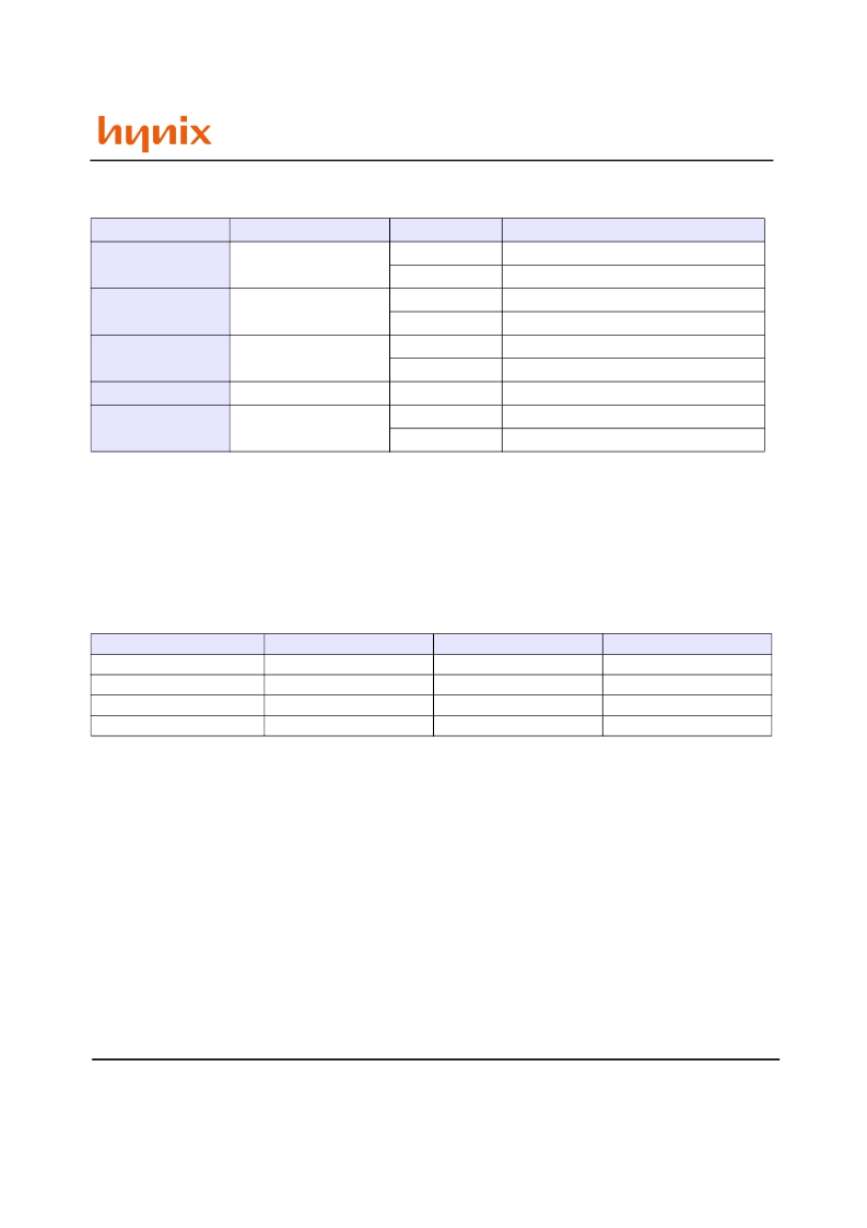
Table 6: Status Register Bit
Read Electronic Signature
The device contains a Manufacturer Code and Device Code. To read these codes two steps are required:
1. first use one Bus Write cycle to issue the Read Electronic Signature command (90h)
2. then subsequent Bus Read operations will read the Manufacturer Code and the Device Code until another command
is issued.
Refer to Table, Read Electronic Signature for information on the addresses.
Automatic Page 0 Read at Power-Up
Automatic Page 0 Read at Power-Up is an option available on all devices belonging to the NAND Flash 528 Byte/264
Word Page family. It allows the microcontroller to directly download boot code from page 0, without requiring any
command or address input sequence. The Automatic Page 0 Read option is particularly suited for applications that
boot from the NAND.
Devices delivered with Automatic Page 0 Read at Power-Up can have the Sequential Row Read option either enabled
ordisabled.
Automatic Page 0 Read Description.
At powerup, once the supply voltage has reached the threshold level, V
CCth
, all digital outputs revert to their reset
state and the internal NAND device functions (reading, writing, erasing) are enabled.
The device then automatically switches to read mode where, as in any read operation, the device is busy for a time
t
BLBH1
during the data is transferred to the Page Buffer. Once the data transfer is complete the Ready/Busy signal goes
High. The data can then be read out sequentially on the I/O bus by pulsing the Read Enable, RE#, signal. Figures 18
and 19 show the power-up waveforms for devices featuring the Automatic Page 0 Read option.
Bit
NAME
Logic Level
Definition
SR7
Write Protection
'1'
Not Protected
'0'
Protected
SR6
Program/Erase/Read
Controller
'1'
P/E/R C Inactive, device ready
'0'
P/E/R C active, device busy
SR5
Program/ Erase/ Read
Controller
'1'
P/E/R C inactive, device ready
'0'
P/E/R C active, device busy
SR4, SR3, SR2
Reserved
Don
'
t Care
SR0
Generic Error
'1'
Error - Operation failed
'0'
No Error - Operation successful
Part Number
Manufacture Code
Device Code
Bus Width
HY27US08121M
ADh
76h
x8
HY27SS08121M
ADh
36h
x8
HY27US16121M
00ADh
0056h
x16
HY27SS16121M
00ADh
0046h
x16
相關PDF資料 |
PDF描述 |
|---|---|
| HY27US16121M | 512Mbit (64Mx8bit / 32Mx16bit) NAND Flash |
| HY29F002TC-70 | 2 Megabit (256K x 8), 5 Volt-only, Flash Memory |
| HY29F002TC-45 | 2 Megabit (256K x 8), 5 Volt-only, Flash Memory |
| HY29F002TC-55 | 2 Megabit (256K x 8), 5 Volt-only, Flash Memory |
| HY29F002T | 2 Megabit (256K x 8), 5 Volt-only, Flash Memory |
相關代理商/技術參數(shù) |
參數(shù)描述 |
|---|---|
| HY29DL162 | 制造商:未知廠家 制造商全稱:未知廠家 功能描述:16M(X8/X16)|3.0V DUAL BANK|70|NOR FLASH - 16M |
| HY29DL162BF-12 | 制造商:HYNIX 制造商全稱:Hynix Semiconductor 功能描述:16 Megabit (2M x 8/1M x16) Low Voltage, Dual Bank, Simultaneous Read/Write Flash Memory |
| HY29DL162BF-12I | 制造商:HYNIX 制造商全稱:Hynix Semiconductor 功能描述:16 Megabit (2M x 8/1M x16) Low Voltage, Dual Bank, Simultaneous Read/Write Flash Memory |
| HY29DL162BF-70 | 制造商:HYNIX 制造商全稱:Hynix Semiconductor 功能描述:16 Megabit (2M x 8/1M x16) Low Voltage, Dual Bank, Simultaneous Read/Write Flash Memory |
| HY29DL162BF-70I | 制造商:HYNIX 制造商全稱:Hynix Semiconductor 功能描述:16 Megabit (2M x 8/1M x16) Low Voltage, Dual Bank, Simultaneous Read/Write Flash Memory |
發(fā)布緊急采購,3分鐘左右您將得到回復。