- 您現(xiàn)在的位置:買賣IC網(wǎng) > PDF目錄373087 > K9F2G08U0M (SAMSUNG SEMICONDUCTOR CO. LTD.) Connector; Leaded Process Compatible:Yes RoHS Compliant: Yes PDF資料下載
參數(shù)資料
| 型號(hào): | K9F2G08U0M |
| 廠商: | SAMSUNG SEMICONDUCTOR CO. LTD. |
| 英文描述: | Connector; Leaded Process Compatible:Yes RoHS Compliant: Yes |
| 中文描述: | 閃存 |
| 文件頁(yè)數(shù): | 30/38頁(yè) |
| 文件大?。?/td> | 601K |
| 代理商: | K9F2G08U0M |
第1頁(yè)第2頁(yè)第3頁(yè)第4頁(yè)第5頁(yè)第6頁(yè)第7頁(yè)第8頁(yè)第9頁(yè)第10頁(yè)第11頁(yè)第12頁(yè)第13頁(yè)第14頁(yè)第15頁(yè)第16頁(yè)第17頁(yè)第18頁(yè)第19頁(yè)第20頁(yè)第21頁(yè)第22頁(yè)第23頁(yè)第24頁(yè)第25頁(yè)第26頁(yè)第27頁(yè)第28頁(yè)第29頁(yè)當(dāng)前第30頁(yè)第31頁(yè)第32頁(yè)第33頁(yè)第34頁(yè)第35頁(yè)第36頁(yè)第37頁(yè)第38頁(yè)
FLASH MEMORY
30
Preliminary
K9F2G08Q0M K9F2G16Q0M
K9F2G08U0M K9F2G16U0M
Device Operation
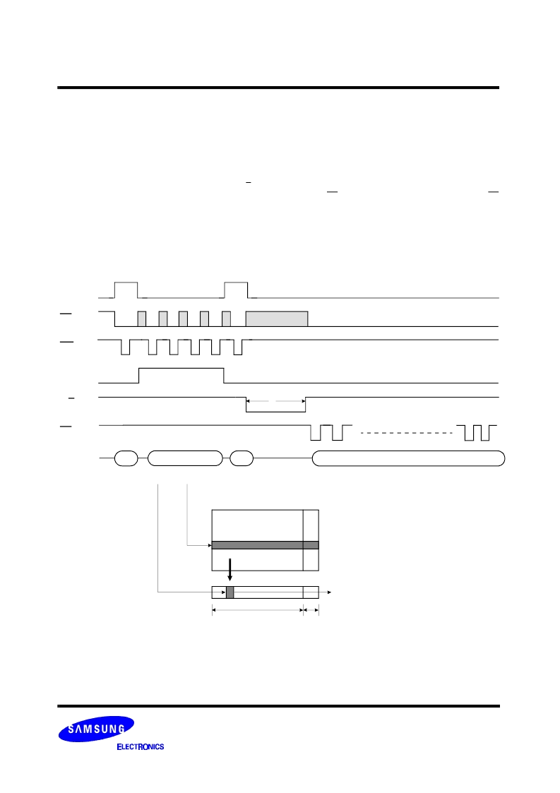
PAGE READ
Upon initial device power up, the device defaults to Read mode. This operation is also initiated by writing 00h-30h to the command
register along with five address cycles. In two consecutive read operations, the second one doesn’t need 00h command, which five
address cycles and 30h command initiates that operation. Once the command is latched, it does not need to be written for the follow-
ing page read operation. Two types of operations are available : random read, serial page read .
The random read mode is enabled when the page address is changed. The 2112 bytes(X8 device) or 1056 words(X16 device) of
data within the selected page are transferred to the data registers in less than 25
μ
s(t
R
). The system controller can detect the comple-
tion of this data transfer(tR) by analyzing the output of R/B pin. Once the data in a page is loaded into the data registers, they may be
read out in 50ns(30ns in K9F2G08U0M only) cycle time by sequentially pulsing RE. The repetitive high to low transitions of the RE
clock make the device output the data starting from the selected column address up to the last column address.
The device may output random data in a page instead of the consecutive sequential data by writing random data output command.
The column address of next data, which is going to be out, may be changed to the address which follows random data output com-
mand. Random data output can be operated multiple times regardless of how many times it is done in a page.
Figure 6. Read Operation
Address(5Cycle)
00h
Col Add1,2 & Row Add1,2,3
Data Output(Serial Access)
Data Field
Spare Field
CE
CLE
ALE
R/B
WE
RE
t
R
30h
I/Ox
相關(guān)PDF資料 |
PDF描述 |
|---|---|
| K9F2G16U0M | FLASH MEMORY |
| K9F2G08Q0M | FLASH MEMORY |
| K9F2G16Q0M | FLASH MEMORY |
| K9F5608D0C | TV 37C 37#16 PIN RECP |
| K9F5616D0C | 32M x 8 Bit , 16M x 16 Bit NAND Flash Memory |
相關(guān)代理商/技術(shù)參數(shù) |
參數(shù)描述 |
|---|---|
| K9F2G08U0M-PCB000 | 制造商:Samsung Semiconductor 功能描述: |
| K9F2G08U0M-PCB0T00 | 制造商:Samsung Semiconductor 功能描述: |
| K9F2G08U0M-PIB0000 | 制造商:Samsung 功能描述:2GB SLC NORMAL X8 TSOP1 - Trays |
| K9F2G08U0M-YCB0 | 制造商:Samsung Electro-Mechanics 功能描述:NAND Flash, 256M x 8, 48 Pin, Plastic, TSSOP |
| K9F2G08UOC-SCBOT00 | 制造商:Samsung SDI 功能描述: |
發(fā)布緊急采購(gòu),3分鐘左右您將得到回復(fù)。