- 您現(xiàn)在的位置:買賣IC網(wǎng) > PDF目錄367540 > LCK4950 Low-Voltage PLL Clock Driver PDF資料下載
參數(shù)資料
| 型號: | LCK4950 |
| 英文描述: | Low-Voltage PLL Clock Driver |
| 中文描述: | 低電壓PLL時鐘驅(qū)動器 |
| 文件頁數(shù): | 11/16頁 |
| 文件大小: | 215K |
| 代理商: | LCK4950 |

Agere Systems Inc.
11
Data Sheet
November 2001
Low-Voltage PLL Clock Driver
LCK4950
Electrical Characteristics
(continued)
5-9707 (F)
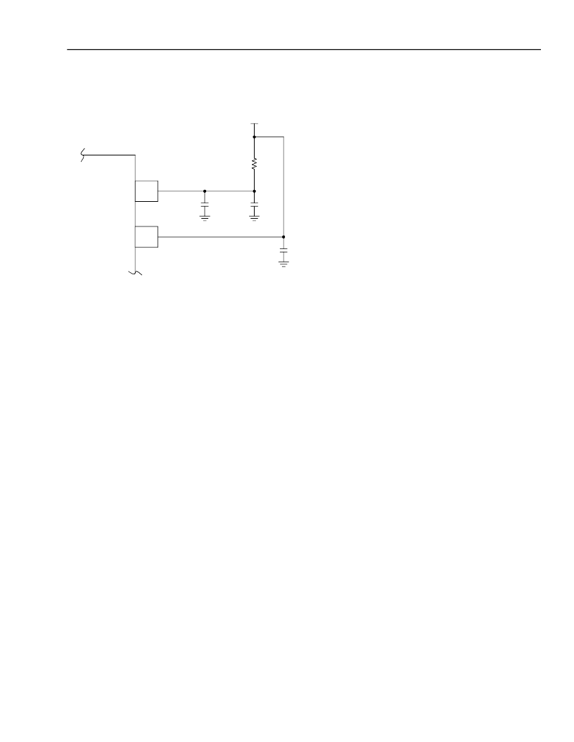
Figure 8. Power Supply Filter
PLL jitter can be measured for configurations where
the outputs are switching at different frequencies by
triggering the lowest-frequency output. PLL jitter is
dependent on internal V
CO
frequency more so than
output configuration.
There are some general guidelines that will minimize
the output jitter of the device. First, always configure
the device so the V
CO
runs as fast as possible. This is
the most important aspect in minimizing jitter of the
LCK4950. Second, maintain the reference frequency at
the highest possible frequency. These more frequent
phase detector updates help to reduce jitter. There is a
trade-off between higher reference frequencies and
higher V
CO
frequency; always choose a higher V
CO
frequency to reduce jitter. Third, and the most difficult
to follow, minimize the number of different frequencies
sourced from a single chip. The fixed edge
displacement associated with the switching noise, in
most cases, nearly doubles the effective jitter of a high-
speed output.
Power Supply Filtering
The LCK4950 exhibits some sensitivities that would not
be seen on a fully digital product because the LCK4950
is a mixed analog/digital product. Analog circuitry is
naturally sensitive to random noise, most noticeably
when the noise is in the power supply pins. The
LCK4950 provides a separate output buffer power
supply (V
DD
) and phase-locked loop (V
DDA
) power
supply pins. This design isolates the high
switching noise digital outputs from the sensitive
internal analog phase-locked loop. In a controlled
setup (i.e., an evaluation board), this amount of
isolation will suffice. In a digital system, where it is
much more difficult to minimize noise on the power
supplies, an additional level of isolation may be
required. The easiest means of accomplishing this is
by applying a power supply filter on the V
DDA
pin for
the LCK4950.
Figure 8 illustrates a typical power supply filter scheme
for the LCK4950. The device is most greatly affected
by spectral content in the 1 kHz to 1 MHz range, and
therefore needs a filter to target this range. The most
important aspect of this final filter design is the dc
voltage drop between the V
DD
supply and V
DDA
pin.
The I
DDPLL
current (current forced through the V
DDA
pin) is normally 45 mA (55 mA maximum), assuming
that a minimum of 3.0 V must be maintained on the
V
DDA
pin. Very little voltage drop can be tolerated when
a 3.3 V V
DD
supply is used. The resistor shown in
Figure 10 must have a resistance of 5
—
10
to meet
the voltage drop criteria. The RC filter shown provides
a broadband filter with about 100:1 attenuation for
noise, with a spectral content above 20 kHz. As the
noise frequency crosses the series resonant point of an
individual capacitor, its overall impedance begins to
look inductive and therefore increases with increasing
frequency. The parallel capacitor circuit shown in
Figure 11 guarantees that a low- impedance path to
ground exists for frequencies exceeding the bandwidth
of the PLL. It is recommended that the user start with
an 8
—
10
resistor to avoid potential V
DD
drop
problems and only use higher-value resistors when a
higher level of attenuation is needed.
The LCK4950 has several design features to minimize
the susceptibility to power supply noise (isolated power
and grounds and fully differential PLL). Still, there may
be applications in which overall performance is being
degraded due to system power supply noise. The
power supply filter schemes discussed in this section
should be adequate to eliminate power supply noise-
related problems in most designs.
0.01
μ
F
22
μ
F
R
S
=
5
—
10
V
CC
PLL_V
CC
LCK4950
0.01
μ
F
3.3 V
相關(guān)PDF資料 |
PDF描述 |
|---|---|
| LCK4953 | Low-Voltage PLL Clock Driver |
| LCS2W123.3W10 | Analog IC |
| LCS2W1233-10W | Analog IC |
| LCS2W243.3W10 | Analog IC |
| LCS2W2433-10W | Analog IC |
相關(guān)代理商/技術(shù)參數(shù) |
參數(shù)描述 |
|---|---|
| LCK4953 | 制造商:AGERE 制造商全稱:AGERE 功能描述:Low-Voltage PLL Clock Driver |
| LCK4972 | 制造商:AGERE 制造商全稱:AGERE 功能描述:Low-Voltage PLL Clock Driver |
| LCK4973 | 制造商:AGERE 制造商全稱:AGERE 功能描述:Low-Voltage PLL Clock Driver |
| LCK4993 | 制造商:AGERE 制造商全稱:AGERE 功能描述:Low-Voltage PLL Clock Drivers |
| LCK4993KB-DB | 制造商:AGERE 制造商全稱:AGERE 功能描述:Low-Voltage PLL Clock Drivers |
發(fā)布緊急采購,3分鐘左右您將得到回復。