- 您現(xiàn)在的位置:買賣IC網(wǎng) > PDF目錄224506 > MT58L512L18PS-7.5IT 512K X 18 CACHE SRAM, 4 ns, PQFP100 PDF資料下載
參數(shù)資料
| 型號(hào): | MT58L512L18PS-7.5IT |
| 元件分類: | SRAM |
| 英文描述: | 512K X 18 CACHE SRAM, 4 ns, PQFP100 |
| 封裝: | PLASTIC, MS-026BHA, TQFP-100 |
| 文件頁數(shù): | 11/32頁 |
| 文件大小: | 616K |
| 代理商: | MT58L512L18PS-7.5IT |
第1頁第2頁第3頁第4頁第5頁第6頁第7頁第8頁第9頁第10頁當(dāng)前第11頁第12頁第13頁第14頁第15頁第16頁第17頁第18頁第19頁第20頁第21頁第22頁第23頁第24頁第25頁第26頁第27頁第28頁第29頁第30頁第31頁第32頁
19
8Mb: 512K x 18, 256K x 32/36 Pipelined, SCD SyncBurst SRAM
Micron Technology, Inc., reserves the right to change products or specifications without notice.
MT58L512L18P_2.p65 – Rev. 6/01
2001, Micron Technology, Inc.
8Mb: 512K x 18, 256K x 32/36
PIPELINED, SCD SYNCBURST SRAM
ABSOLUTE MAXIMUM RATINGS*
Voltage on VDD Supply
Relative to VSS .............................. -0.5V to +4.6V
Voltage on VDDQ Supply
Relative to VSS .............................. -0.5V to +4.6V
VIN (DQx) .................................. -0.5V to VDDQ + 0.5V
VIN (inputs) ................................... -0.5V to VDD + 0.5V
Storage Temperature (plastic) ............ -55°C to +150°C
Storage Temperature (FBGA) ............. -55°C to +125°C
Junction Temperature** ................................... +150°C
Short Circuit Output Current .......................... 100mA
*Stresses greater than those listed under “Absolute
Maximum Ratings” may cause permanent damage to
the device. This is a stress rating only, and functional
operation of the device at these or any other
conditions above those indicated in the operational
sections of this specification is not implied. Exposure
to absolute maximum rating conditions for extended
periods may affect reliability.
**Maximum junction temperature depends upon
package type, cycle time, loading, ambient tempera-
ture and airflow. See Micron Technical Note TN-05-
14 for more information.
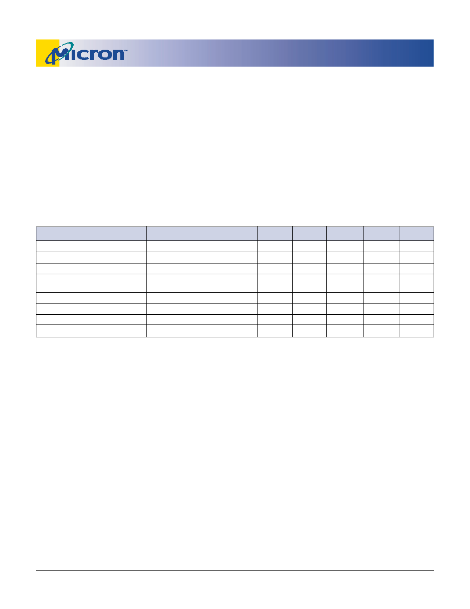
3.3V I/O DC ELECTRICAL CHARACTERISTICS AND OPERATING CONDITIONS
(0°C
≤ T
A ≤ +70°C; VDD, VDDQ = +3.3V +0.3V/-0.165V unless otherwise noted)
DESCRIPTION
CONDITIONS
SYMBOL
MIN
MAX
UNITS
NOTES
Input High (Logic 1) Voltage
VIH
2.0
VDD + 0.3
V
1, 2
Input Low (Logic 0) Voltage
VIL
-0.3
0.8
V
1, 2
Input Leakage Current
0V
≤ VIN ≤ VDD
ILI
-1.0
1.0
A
3
Output Leakage Current
Output(s) disabled,
ILO
-1.0
1.0
A
0V
≤ VIN ≤ VDD
Output High Voltage
IOH = -4.0mA
VOH
2.4
–
V
1, 4
Output Low Voltage
IOL = 8.0mA
VOL
–
0.4
V
1, 4
Supply Voltage
VDD
3.135
3.6
V
1
Isolated Output Buffer Supply
VDDQ
3.135
3.6
V
1, 5
NOTE: 1. All voltages referenced to VSS (GND).
2. Overshoot:
VIH
≤ +4.6V for t ≤ tKC/2 for I ≤ 20mA
Undershoot:
VIL
≥ -0.7V for t ≤ tKC/2 for I ≤ 20mA
Power-up:
VIH
≤ +3.6V and VDD ≤ 3.135V for t ≤ 200ms
3. MODE has an internal pull-up, and input leakage = ±10A.
4. The load used for VOH, VOL testing is shown in Figure 2 for 3.3V I/O. AC load current is higher than the shown DC
values. AC I/O curves are available upon request.
5. VDDQ should never exceed VDD. VDD and VDDQ can be connected together.
相關(guān)PDF資料 |
PDF描述 |
|---|---|
| MT78740 | RELAY SOCKET |
| MT78745 | RELAY SOCKET |
| MT9KDF12872PZ-1G6XX | 128M X 72 DDR DRAM MODULE, DMA240 |
| MTE-28-T | INTERCONNECTION DEVICE |
| MTE-11-T | INTERCONNECTION DEVICE |
相關(guān)代理商/技術(shù)參數(shù) |
參數(shù)描述 |
|---|---|
| MT58L512L18PT-10 | 制造商:Cypress Semiconductor 功能描述:512KX18 SRAM PLASTIC TQFP 3.3V 制造商:Rochester Electronics LLC 功能描述:- Bulk |
| MT58L512L18PT-7.5 | 制造商:Rochester Electronics LLC 功能描述:- Bulk |
| MT58L512L18PT-7.5 IT | 制造商:Cypress Semiconductor 功能描述:512KX18 SRAM PLASTIC IND TEMP |
| MT58L512V18F | 制造商:MICRON 制造商全稱:Micron Technology 功能描述:8Mb: 512K x 18, 256K x 32/36 FLOW-THROUGH SYNCBURST SRAM |
| MT58L512V18P | 制造商:MICRON 制造商全稱:Micron Technology 功能描述:8Mb: 512K x 18, 256K x 32/36 PIPELINED, SCD SYNCBURST SRAM |
發(fā)布緊急采購,3分鐘左右您將得到回復(fù)。