- 您現(xiàn)在的位置:買賣IC網(wǎng) > PDF目錄11733 > ORSO82G5-1FN680I (Lattice Semiconductor Corporation)IC TRANCEIVERS FPSC 680FPBGA PDF資料下載
參數(shù)資料
| 型號: | ORSO82G5-1FN680I |
| 廠商: | Lattice Semiconductor Corporation |
| 文件頁數(shù): | 19/153頁 |
| 文件大小: | 0K |
| 描述: | IC TRANCEIVERS FPSC 680FPBGA |
| 產(chǎn)品變化通告: | Product Discontinuation 01/Aug/2011 |
| 標準包裝: | 24 |
| 系列: | * |
第1頁第2頁第3頁第4頁第5頁第6頁第7頁第8頁第9頁第10頁第11頁第12頁第13頁第14頁第15頁第16頁第17頁第18頁當前第19頁第20頁第21頁第22頁第23頁第24頁第25頁第26頁第27頁第28頁第29頁第30頁第31頁第32頁第33頁第34頁第35頁第36頁第37頁第38頁第39頁第40頁第41頁第42頁第43頁第44頁第45頁第46頁第47頁第48頁第49頁第50頁第51頁第52頁第53頁第54頁第55頁第56頁第57頁第58頁第59頁第60頁第61頁第62頁第63頁第64頁第65頁第66頁第67頁第68頁第69頁第70頁第71頁第72頁第73頁第74頁第75頁第76頁第77頁第78頁第79頁第80頁第81頁第82頁第83頁第84頁第85頁第86頁第87頁第88頁第89頁第90頁第91頁第92頁第93頁第94頁第95頁第96頁第97頁第98頁第99頁第100頁第101頁第102頁第103頁第104頁第105頁第106頁第107頁第108頁第109頁第110頁第111頁第112頁第113頁第114頁第115頁第116頁第117頁第118頁第119頁第120頁第121頁第122頁第123頁第124頁第125頁第126頁第127頁第128頁第129頁第130頁第131頁第132頁第133頁第134頁第135頁第136頁第137頁第138頁第139頁第140頁第141頁第142頁第143頁第144頁第145頁第146頁第147頁第148頁第149頁第150頁第151頁第152頁第153頁
Lattice Semiconductor
ORCA ORSO42G5 and ORSO82G5 Data Sheet
115
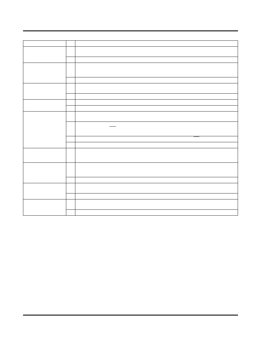
MPI_ACK
O
In
MPI mode this is driven low indicating the MPI received the data on the write cycle or
returned data on a read cycle.
I/O If not used for MPI these pins are user-programmable I/O pins after conguration.
1
MPI_CLK
I
This is the PowerPC synchronous, positive-edge bus clock used for the
MPI interface. It can be
a source of the clock for the Embedded System Bus. If MPI is used this will be the AMBA bus
clock.
I/O If not used for MPI these pins are user-programmable I/O pins after conguration.
1
MPI_TEA
O
A low on the MPI transfer error acknowledge indicates that the MPI detects a bus error on the
internal system bus for the current transaction.
I/O If not used for MPI these pins are user-programmable I/O pins after conguration.
1
MPI_RTRY
O
This pin requests the MPC860 to relinquish the bus and retry the cycle.
I/O If not used for MPI these pins are user-programmable I/O pins after conguration.
1
D[0:31]
I/O Selectable data bu
s width from 8, 16, 32-bit in MPI mode. Driven by the bus master in a write
transaction and driven by MPI in a read transaction.
I
D[7:0] receive conguration data during master parallel, peripheral, and slave parallel congu-
ration modes when WR is low and each pin has a pull-up enabled. During serial conguration
modes, D0 is the DIN input.
O
D[7:3] output internal status for asynchronous peripheral mode when RD is low.
I/O After conguration, if MPI is not used, the pins are user-programmable I/O pins.
1
DP[0:3]
I/O Selectable parity bus width in MPI mode from 1, 2, 4-bit, DP[0] for D[0:7], DP[1] for D[8:15],
DP[2] for D[16:23], and DP[3] for D[24:31].
After conguration, if MPI is not used, the pins are user-programmable I/O pin.
1
DIN
I
During slave serial or master serial conguration modes, DIN accepts serial conguration data
synchronous with CCLK. During parallel conguration modes, DIN is the D0 input. During con-
guration, a pull-up is enabled.
I/O After conguration, this pin is a user-programmable I/O pin.
1
DOUT
O
During conguration, DOUT is the serial data output that can drive the DIN of daisy-chained
slave devices. Data out on DOUT changes on the rising edge of CCLK.
I/O After conguration, DOUT is a user-programmable I/O pin.
1
TESTCFG
(ORSO82G5 only)
I
During conguration this pin should be held high, to allow conguration to occur. A pull up is
enabled during conguration.
I/O After conguration, TESTCFG is a user programmable I/O pin.
1
1. The FPGA States of Operation section in the ORCA Series 4 FPGAs data sheet contains more information on how to control these signals
during start-up. The timing of DONE release is controlled by one set of bit stream options, and the timing of the simultaneous release of all
other conguration pins (and the activation of all user I/Os) is controlled by a second set of options.
Table 47. Pin Descriptions (Continued)
Symbol
I/O
Description
相關PDF資料 |
PDF描述 |
|---|---|
| PIC32MX775F256L-80I/PT | IC MCU 32BIT 256K FLASH 100TQFP |
| VI-J4F-IW-F4 | CONVERTER MOD DC/DC 72V 100W |
| PIC18LF8520-I/PT | IC MCU FLASH 16KX16 EEPROM80TQFP |
| PIC18LF458-I/L | IC MCU CAN FLASH 16K LP 44-PLCC |
| VI-J4F-IW-F2 | CONVERTER MOD DC/DC 72V 100W |
相關代理商/技術參數(shù) |
參數(shù)描述 |
|---|---|
| ORSO82G5-1FN680I1 | 功能描述:FPGA - 現(xiàn)場可編程門陣列 10368 LUT 372 I/O RoHS:否 制造商:Altera Corporation 系列:Cyclone V E 柵極數(shù)量: 邏輯塊數(shù)量:943 內(nèi)嵌式塊RAM - EBR:1956 kbit 輸入/輸出端數(shù)量:128 最大工作頻率:800 MHz 工作電源電壓:1.1 V 最大工作溫度:+ 70 C 安裝風格:SMD/SMT 封裝 / 箱體:FBGA-256 |
| ORSO82G5-2BM680C | 功能描述:FPGA - 現(xiàn)場可編程門陣列 10368 LUT 372 I/O RoHS:否 制造商:Altera Corporation 系列:Cyclone V E 柵極數(shù)量: 邏輯塊數(shù)量:943 內(nèi)嵌式塊RAM - EBR:1956 kbit 輸入/輸出端數(shù)量:128 最大工作頻率:800 MHz 工作電源電壓:1.1 V 最大工作溫度:+ 70 C 安裝風格:SMD/SMT 封裝 / 箱體:FBGA-256 |
| ORSO82G5-2BM680I | 功能描述:FPGA - 現(xiàn)場可編程門陣列 10368 LUT 372 I/O RoHS:否 制造商:Altera Corporation 系列:Cyclone V E 柵極數(shù)量: 邏輯塊數(shù)量:943 內(nèi)嵌式塊RAM - EBR:1956 kbit 輸入/輸出端數(shù)量:128 最大工作頻率:800 MHz 工作電源電壓:1.1 V 最大工作溫度:+ 70 C 安裝風格:SMD/SMT 封裝 / 箱體:FBGA-256 |
| ORSO82G5-2F680C | 功能描述:FPGA - 現(xiàn)場可編程門陣列 ORCA FPSC 2.7Gbits/s BP XCVR 643K RoHS:否 制造商:Altera Corporation 系列:Cyclone V E 柵極數(shù)量: 邏輯塊數(shù)量:943 內(nèi)嵌式塊RAM - EBR:1956 kbit 輸入/輸出端數(shù)量:128 最大工作頻率:800 MHz 工作電源電壓:1.1 V 最大工作溫度:+ 70 C 安裝風格:SMD/SMT 封裝 / 箱體:FBGA-256 |
| ORSO82G5-2F680I | 功能描述:FPGA - 現(xiàn)場可編程門陣列 ORCA FPSC 2.7GBITS/s BP XCVR 643K RoHS:否 制造商:Altera Corporation 系列:Cyclone V E 柵極數(shù)量: 邏輯塊數(shù)量:943 內(nèi)嵌式塊RAM - EBR:1956 kbit 輸入/輸出端數(shù)量:128 最大工作頻率:800 MHz 工作電源電壓:1.1 V 最大工作溫度:+ 70 C 安裝風格:SMD/SMT 封裝 / 箱體:FBGA-256 |
發(fā)布緊急采購,3分鐘左右您將得到回復。