- 您現(xiàn)在的位置:買賣IC網(wǎng) > PDF目錄368232 > PSD834F2 Flash In-System Programmable (ISP) Peripherals For 8-bit MCUs(用于8位MCUs的閃速ISP外圍) PDF資料下載
參數(shù)資料
| 型號: | PSD834F2 |
| 英文描述: | Flash In-System Programmable (ISP) Peripherals For 8-bit MCUs(用于8位MCUs的閃速ISP外圍) |
| 中文描述: | Flash在系統(tǒng)可編程(ISP)為周邊8位微控制器(用于8位微控制器的閃速的ISP外圍) |
| 文件頁數(shù): | 19/98頁 |
| 文件大?。?/td> | 595K |
| 代理商: | PSD834F2 |
第1頁第2頁第3頁第4頁第5頁第6頁第7頁第8頁第9頁第10頁第11頁第12頁第13頁第14頁第15頁第16頁第17頁第18頁當前第19頁第20頁第21頁第22頁第23頁第24頁第25頁第26頁第27頁第28頁第29頁第30頁第31頁第32頁第33頁第34頁第35頁第36頁第37頁第38頁第39頁第40頁第41頁第42頁第43頁第44頁第45頁第46頁第47頁第48頁第49頁第50頁第51頁第52頁第53頁第54頁第55頁第56頁第57頁第58頁第59頁第60頁第61頁第62頁第63頁第64頁第65頁第66頁第67頁第68頁第69頁第70頁第71頁第72頁第73頁第74頁第75頁第76頁第77頁第78頁第79頁第80頁第81頁第82頁第83頁第84頁第85頁第86頁第87頁第88頁第89頁第90頁第91頁第92頁第93頁第94頁第95頁第96頁第97頁第98頁
19/98
PSD8XXF2/3/4/5
Programming Flash Memory
Flash memory must be erased prior to being pro-
grammed. A byte of Flash memory is erased to all
1s (FFh), and is programmed by setting selected
bits to 0. The MCU may erase Flash memory all at
once or by-sector, but not byte-by-byte. However,
the MCU may program Flash memory byte-by-
byte.
The primary and secondary Flash memories re-
quire the MCU to send an instruction to program a
byte or to erase sectors (see Table 8).
Once theMCU issues a Flash memoryProgram or
Erase instruction, it must check for the status bits
for completion. Theembedded algorithms that are
invoked inside the PSD8xxF2/3/4/5support sever-
al means to provide statusto theMCU. Status may
be checked using any of three methods: DataPoll-
ing, Data Toggle, or Ready/Busy (PC3).
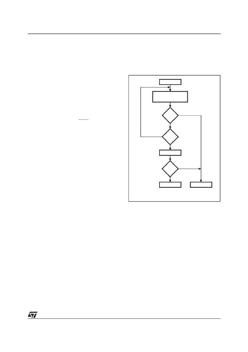
Data Polling.
Polling on the Data Polling Flag
(DQ7) bit is a method of checking whether a Pro-
gram orErase cycle is in progress or has complet-
ed. Figure 4 shows the Data Polling algorithm.
When the MCU issues a Program instruction, the
embedded algorithm within the PSD8xxF2/3/4/5
begins. The MCU then reads the location of the
byte to be programmed in Flash memory to check
status. The Data Polling Flag (DQ7) bit of this lo-
cation becomes the complement of b7 of the orig-
inal data byte to be programmed. The MCU
continues to poll this location, comparing the Data
Polling Flag (DQ7) bit and monitoring the Error
Flag (DQ5)bit. When the Data Polling Flag (DQ7)
bit matches b7 of the original data, and the Error
Flag (DQ5) bit remains 0, the embedded algorithm
is complete. If the Error Flag (DQ5) bit is 1, the
MCU should test the Data Polling Flag (DQ7) bit
again since the Data Polling Flag (DQ7) bit may
have changed simultaneously with the Error Flag
(DQ5) bit (see Figure 4).
The Error Flag (DQ5) bit is set if either an internal
time-out occurred while the embedded algorithm
attempted to program the byte or if the MCU at-
tempted toprogram a 1 to a bit that was not erased
(not erased is logic 0).
It issuggested (as withall Flash memories)to read
the location again after the embedded program-
ming algorithm has completed, to compare the
byte that was written to the Flash memory with the
byte that was intended to be written.
When using the Data Polling method during an
Erase cycle, Figure 4 still applies. However, the
Data Polling Flag (DQ7) bit is 0 until the Erase cy-
cle is complete. A 1 on the Error Flag (DQ5) bit in-
dicates a time-out condition on the Erase cycle; a
0 indicates no error. The MCU can read any loca-
tion within the sector being erased to get the Data
Polling Flag (DQ7) bit andthe Error Flag (DQ5)bit.
PSDsoft Express generates ANSI C code func-
tions which implement these Data Polling algo-
rithms.
Figure 4. Data Polling Flowchart
Data Toggle.
Checking the Toggle Flag (DQ6) bit
is a method of determining whether a Program or
Erase cycle is in progress or has completed. Fig-
ure 5 shows the Data Toggle algorithm.
When the MCU issues a Program instruction, the
embedded algorithm within the PSD8xxF2/3/4/5
begins. The MCU then reads the location of the
byte to beprogrammed in Flash memory to check
status. The Toggle Flag (DQ6) bit of this location
toggles eachtime theMCU reads this location until
the embedded algorithm is complete. The MCU
continues to read this location, checking the Tog-
gle Flag (DQ6) bit and monitoring the Error Flag
(DQ5) bit. When the Toggle Flag (DQ6) bit stops
toggling (two consecutive reads yield the same
value), and the Error Flag (DQ5) bit remains 0, the
embedded algorithm is complete. If the Error Flag
(DQ5) bit is 1, the MCU should test the Toggle
Flag (DQ6) bit again, since the Toggle Flag (DQ6)
bit may have changed simultaneously with the Er-
ror Flag (DQ5) bit (see Figure 5).
READ DQ5 &
DQ7
at VALID ADDRESS
START
READ DQ7
FAIL
PASS
AI01369B
DQ7
DATA
YES
NO
YES
NO
DQ5
= 1
DQ7
DATA
YES
NO
相關PDF資料 |
PDF描述 |
|---|---|
| PSD835G2 | Configurable Memory System on a Chip for 8-Bit Microcontrollers(8位微控制器片上存儲器可編程外設) |
| PSD835G2 | 100V 100kRad Hi-Rel Single N-Channel TID Hardened MOSFET in a TO-254AA Tabless package; Similar to IRHMJ57160 with optional Total Dose Rating of 1000kRads |
| PSD835G2V | 150V 100kRad Hi-Rel Single N-Channel TID Hardened MOSFET in a SMD-2 package. Also available with 300 kRads Total Dose Rating.; Similar to IRHNA67164 with optional Total Dose Rating of 300 kRads. |
| PSD835G2-B-12B81 | Configurable Memory System on a Chip for 8-Bit Microcontrollers |
| PSD835F2-B-12B81 | Configurable Memory System on a Chip for 8-Bit Microcontrollers |
相關代理商/技術(shù)參數(shù) |
參數(shù)描述 |
|---|---|
| PSD834F2-15M | 制造商:STMicroelectronics 功能描述:Flash In-System Programmable Peripherals 52-Pin PQFP |
| PSD834F2-70J | 功能描述:CPLD - 復雜可編程邏輯器件 5.0V 2M 70ns RoHS:否 制造商:Lattice 系列: 存儲類型:EEPROM 大電池數(shù)量:128 最大工作頻率:333 MHz 延遲時間:2.7 ns 可編程輸入/輸出端數(shù)量:64 工作電源電壓:3.3 V 最大工作溫度:+ 90 C 最小工作溫度:0 C 封裝 / 箱體:TQFP-100 |
| PSD834F2-70M | 功能描述:SPLD - 簡單可編程邏輯器件 5.0V 2M 70ns RoHS:否 制造商:Texas Instruments 邏輯系列:TICPAL22V10Z 大電池數(shù)量:10 最大工作頻率:66 MHz 延遲時間:25 ns 工作電源電壓:4.75 V to 5.25 V 電源電流:100 uA 最大工作溫度:+ 75 C 最小工作溫度:0 C 安裝風格:Through Hole 封裝 / 箱體:DIP-24 |
| PSD834F2-90J | 功能描述:CPLD - 復雜可編程邏輯器件 5.0V 2M 90ns RoHS:否 制造商:Lattice 系列: 存儲類型:EEPROM 大電池數(shù)量:128 最大工作頻率:333 MHz 延遲時間:2.7 ns 可編程輸入/輸出端數(shù)量:64 工作電源電壓:3.3 V 最大工作溫度:+ 90 C 最小工作溫度:0 C 封裝 / 箱體:TQFP-100 |
| PSD834F2-90JI | 功能描述:CPLD - 復雜可編程邏輯器件 5.0V 2M 90ns RoHS:否 制造商:Lattice 系列: 存儲類型:EEPROM 大電池數(shù)量:128 最大工作頻率:333 MHz 延遲時間:2.7 ns 可編程輸入/輸出端數(shù)量:64 工作電源電壓:3.3 V 最大工作溫度:+ 90 C 最小工作溫度:0 C 封裝 / 箱體:TQFP-100 |
發(fā)布緊急采購,3分鐘左右您將得到回復。