- 您現(xiàn)在的位置:買賣IC網(wǎng) > PDF目錄368232 > PSD834F2 Flash In-System Programmable (ISP) Peripherals For 8-bit MCUs(用于8位MCUs的閃速ISP外圍) PDF資料下載
參數(shù)資料
| 型號: | PSD834F2 |
| 英文描述: | Flash In-System Programmable (ISP) Peripherals For 8-bit MCUs(用于8位MCUs的閃速ISP外圍) |
| 中文描述: | Flash在系統(tǒng)可編程(ISP)為周邊8位微控制器(用于8位微控制器的閃速的ISP外圍) |
| 文件頁數(shù): | 49/98頁 |
| 文件大?。?/td> | 595K |
| 代理商: | PSD834F2 |
第1頁第2頁第3頁第4頁第5頁第6頁第7頁第8頁第9頁第10頁第11頁第12頁第13頁第14頁第15頁第16頁第17頁第18頁第19頁第20頁第21頁第22頁第23頁第24頁第25頁第26頁第27頁第28頁第29頁第30頁第31頁第32頁第33頁第34頁第35頁第36頁第37頁第38頁第39頁第40頁第41頁第42頁第43頁第44頁第45頁第46頁第47頁第48頁當(dāng)前第49頁第50頁第51頁第52頁第53頁第54頁第55頁第56頁第57頁第58頁第59頁第60頁第61頁第62頁第63頁第64頁第65頁第66頁第67頁第68頁第69頁第70頁第71頁第72頁第73頁第74頁第75頁第76頁第77頁第78頁第79頁第80頁第81頁第82頁第83頁第84頁第85頁第86頁第87頁第88頁第89頁第90頁第91頁第92頁第93頁第94頁第95頁第96頁第97頁第98頁
49/98
PSD8XXF2/3/4/5
Direction Register.
The Direction Register, in
conjunction with the output enable (except for Port
D), controls the direction of data flow in the I/O
Ports. Any bit set to 1 in the Direction Register
causes the corresponding pin to be an output, and
any bitset to0 causes itto be aninput. The default
mode for all port pins is input.
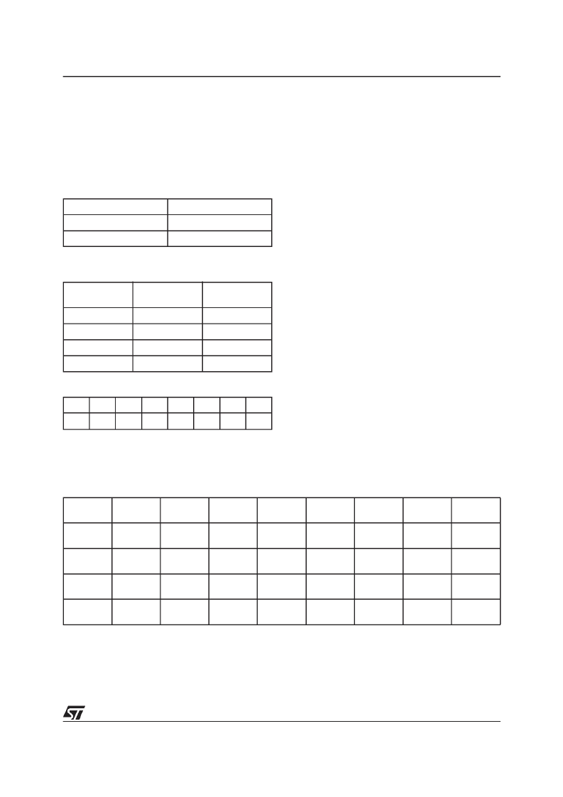
Table 23. Port Pin Direction Control, Output
Enable P.T. Not Defined
Table 24. Port Pin Direction Control, Output
Enable P.T. Defined
Table 25. Port Direction Assignment Example
Figure 25 and Figure 26 show the Port Architec-
ture diagrams for Ports A/B and C, respectively.
The direction of data flow for Ports A,B, and C are
controlled not only by the direction register, but
also by the output enable product term from the
PLD AND Array. If the output enable product term
is not active, the Direction Register has sole con-
trol of a given pin’s direction.
An example of a configuration for a Port with the
three leastsignificant bits set tooutput and the re-
mainder set to input is shown in Table 25. Since
Port D only contains three pins (shown in Figure
28), the Direction Register for Port D has only the
three least significant bits active.
Drive Select Register.
The DriveSelect Register
configures the pin driver as Open Drain or CMOS
for some port pins, and controls the slew rate for
the other port pins. An external pull-up resistor
should be usedfor pins configuredas Open Drain.
A pin can be configured as Open Drain if its corre-
sponding bit in the Drive Select Register is set to a
1. The default pin drive is CMOS.
Note that the slew rate is a measurement of the
rise and fall times of an output. A higher slew rate
means a faster output response and may create
more electrical noise. A pin operates in a high slew
rate when the corresponding bit in the Drive Reg-
ister is set to 1. The default rate is slow slew.
Table 26 shows the Drive Register for Ports A, B,
C, and D. It summarizes which pins can be config-
ured as Open Drain outputs and which pins the
slew rate can be set for.
Port Data Registers
The Port Data Registers, shown in Table 27, are
used by the MCU to writedata to or read data from
the ports. Table 27 shows the register name, the
ports having each register type, and MCU access
for each register type. The registers are described
below.
Table 26. Drive Register Pin Assignment
Note: 1. NA = Not Applicable.
Direction Register Bit
Port Pin Mode
0
Input
1
Output
Direction
Register Bit
Output Enable
P.T.
Port Pin Mode
0
0
Input
0
1
Output
1
0
Output
1
1
Output
Bit 7
Bit 6
Bit 5
Bit 4
Bit 3
Bit 2
Bit 1
Bit 0
0
0
0
0
0
1
1
1
Drive
Register
Bit 7
Bit 6
Bit 5
Bit 4
Bit 3
Bit 2
Bit 1
Bit 0
Port A
Open
Drain
Open
Drain
Open
Drain
Open
Drain
Slew
Rate
Slew
Rate
Slew
Rate
Slew
Rate
Port B
Open
Drain
Open
Drain
Open
Drain
Open
Drain
Slew
Rate
Slew
Rate
Slew
Rate
Slew
Rate
Port C
Open
Drain
Open
Drain
Open
Drain
Open
Drain
Open
Drain
Open
Drain
Open
Drain
Open
Drain
Port D
NA
1
NA
1
NA
1
NA
1
NA
1
Slew
Rate
Slew
Rate
Slew
Rate
相關(guān)PDF資料 |
PDF描述 |
|---|---|
| PSD835G2 | Configurable Memory System on a Chip for 8-Bit Microcontrollers(8位微控制器片上存儲器可編程外設(shè)) |
| PSD835G2 | 100V 100kRad Hi-Rel Single N-Channel TID Hardened MOSFET in a TO-254AA Tabless package; Similar to IRHMJ57160 with optional Total Dose Rating of 1000kRads |
| PSD835G2V | 150V 100kRad Hi-Rel Single N-Channel TID Hardened MOSFET in a SMD-2 package. Also available with 300 kRads Total Dose Rating.; Similar to IRHNA67164 with optional Total Dose Rating of 300 kRads. |
| PSD835G2-B-12B81 | Configurable Memory System on a Chip for 8-Bit Microcontrollers |
| PSD835F2-B-12B81 | Configurable Memory System on a Chip for 8-Bit Microcontrollers |
相關(guān)代理商/技術(shù)參數(shù) |
參數(shù)描述 |
|---|---|
| PSD834F2-15M | 制造商:STMicroelectronics 功能描述:Flash In-System Programmable Peripherals 52-Pin PQFP |
| PSD834F2-70J | 功能描述:CPLD - 復(fù)雜可編程邏輯器件 5.0V 2M 70ns RoHS:否 制造商:Lattice 系列: 存儲類型:EEPROM 大電池?cái)?shù)量:128 最大工作頻率:333 MHz 延遲時間:2.7 ns 可編程輸入/輸出端數(shù)量:64 工作電源電壓:3.3 V 最大工作溫度:+ 90 C 最小工作溫度:0 C 封裝 / 箱體:TQFP-100 |
| PSD834F2-70M | 功能描述:SPLD - 簡單可編程邏輯器件 5.0V 2M 70ns RoHS:否 制造商:Texas Instruments 邏輯系列:TICPAL22V10Z 大電池?cái)?shù)量:10 最大工作頻率:66 MHz 延遲時間:25 ns 工作電源電壓:4.75 V to 5.25 V 電源電流:100 uA 最大工作溫度:+ 75 C 最小工作溫度:0 C 安裝風(fēng)格:Through Hole 封裝 / 箱體:DIP-24 |
| PSD834F2-90J | 功能描述:CPLD - 復(fù)雜可編程邏輯器件 5.0V 2M 90ns RoHS:否 制造商:Lattice 系列: 存儲類型:EEPROM 大電池?cái)?shù)量:128 最大工作頻率:333 MHz 延遲時間:2.7 ns 可編程輸入/輸出端數(shù)量:64 工作電源電壓:3.3 V 最大工作溫度:+ 90 C 最小工作溫度:0 C 封裝 / 箱體:TQFP-100 |
| PSD834F2-90JI | 功能描述:CPLD - 復(fù)雜可編程邏輯器件 5.0V 2M 90ns RoHS:否 制造商:Lattice 系列: 存儲類型:EEPROM 大電池?cái)?shù)量:128 最大工作頻率:333 MHz 延遲時間:2.7 ns 可編程輸入/輸出端數(shù)量:64 工作電源電壓:3.3 V 最大工作溫度:+ 90 C 最小工作溫度:0 C 封裝 / 箱體:TQFP-100 |
發(fā)布緊急采購,3分鐘左右您將得到回復(fù)。