- 您現(xiàn)在的位置:買賣IC網(wǎng) > PDF目錄373223 > R2061K real-time clock ICs PDF資料下載
參數(shù)資料
| 型號: | R2061K |
| 英文描述: | real-time clock ICs |
| 中文描述: | 實時時鐘IC |
| 文件頁數(shù): | 20/48頁 |
| 文件大小: | 322K |
| 代理商: | R2061K |
第1頁第2頁第3頁第4頁第5頁第6頁第7頁第8頁第9頁第10頁第11頁第12頁第13頁第14頁第15頁第16頁第17頁第18頁第19頁當(dāng)前第20頁第21頁第22頁第23頁第24頁第25頁第26頁第27頁第28頁第29頁第30頁第31頁第32頁第33頁第34頁第35頁第36頁第37頁第38頁第39頁第40頁第41頁第42頁第43頁第44頁第45頁第46頁第47頁第48頁
R2061 Series
I
Interfacing with the CPU
G
DATA TRANSFER FORMATS
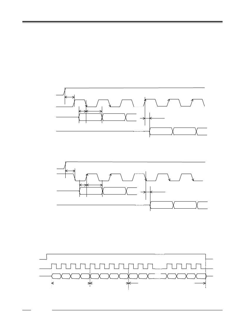
(1) Timing Between CE Pin Transition and Data Input / Output
The R2061 adopts a 3-wire serial interface by which they use the CE (Chip Enable), SCLK (Serial Clock), and SIO
(Serial Input/Output) pins to receive and send data to and from the CPU. The 3-wire serial interface provides two
types of input/output timings with which the SIO pin output and input are synchronized with the rising or falling
edges of the SCLK pin input, respectively, and vice versa. The R2061 is configured to select either one of two
different input/output timings depending on the level of the SCLK pin in the low to high transition of the CE pin.
Namely, when the SCLK pin is held low in the low to high transition of the CE pin, the models will select the timing
with which the SIO pin output is synchronized with the rising edge of the SCLK pin input, and the input is
synchronized with the falling edge of the SCLK pin input, as illustrated in the timing chart below.
12345
Rev.1.00 - 20 -
SCLK
SIO (for reading)
t
DS
SIO (for writing)
CE
t
CES
t
DH
t
RD
Conversely, when the SCLK pin is held high in the low to high transition of the CE pin, the models will select the
timing with which the SIO pin output is synchronized with the falling edge of the SCLK pin input, and the input is
synchronized with the rising edge of the SCLK pin input, as illustrated in the timing chart below.
SCLK
SIO (for reading)
t
DS
SIO (for writing)
CE
t
CES
t
DH
t
RD
(2) Data Transfer Formats
Data transfer is commenced in the low to high transition of the CE pin input and completed in its high to low
transition. Data transfer is conducted serially in multiple units of 1 byte (8 bits). The former 4 bits are used to
specify in the Address Pointer a head address with which data transfer is to be commenced from the host. The
latter 4 bits are used to select either reading data transfer or writing data transfer, and to set the Transfer Format
Register to specify an appropriate data transfer format. All data transfer formats are designed to transfer the most
significant bit (MSB) first.
A2
CE
SCLK
6
A1
A0
C3
C2
C1
C0
A3
7
5
8
2
3
1
2
3
1
4
D7
D6
D3
D2
D1
D0
Setting
the Address Pointer
Writing or Reading data transfer
Setting the Transfer
Format Register
SIO
Two types of data transfer formats are available for reading data transfer and writing data transfer each.
相關(guān)PDF資料 |
PDF描述 |
|---|---|
| R209408012 | SOCKET MMS SURFACE MOUNT |
| R295000062 | LEAD RG316 MMS R/A 0.2M |
| R295000063 | LEAD RG178 MMS R/A 0.2M |
| R210A | Optoelectronic |
| R210B | Optoelectronic |
相關(guān)代理商/技術(shù)參數(shù) |
參數(shù)描述 |
|---|---|
| R2061K01-E2 | 制造商:RICOH 制造商全稱:RICOH electronics devices division 功能描述:wire interface Real-Time Clock ICs with Battery Backup switch-over Function |
| R2061K03-E2 | 制造商:RICOH 制造商全稱:RICOH electronics devices division 功能描述:wire interface Real-Time Clock ICs with Battery Backup switch-over Function |
| R2061S02-E2 | 制造商:RICOH 制造商全稱:RICOH electronics devices division 功能描述:wire interface Real-Time Clock ICs with Battery Backup switch-over Function |
| R2062 | 制造商:RICOH 制造商全稱:RICOH electronics devices division 功能描述:3 wire interface Real-Time Clock ICs with Battery Backup switch-over Function |
| R2062K01-E2 | 制造商:RICOH 制造商全稱:RICOH electronics devices division 功能描述:3 wire interface Real-Time Clock ICs with Battery Backup switch-over Function |
發(fā)布緊急采購,3分鐘左右您將得到回復(fù)。