- 您現(xiàn)在的位置:買賣IC網(wǎng) > PDF目錄376355 > SLB128B (National Semiconductor Corporation) Transmitter with built-in scaler for LVDS Display Interface (LDI) PDF資料下載
參數(shù)資料
| 型號: | SLB128B |
| 廠商: | National Semiconductor Corporation |
| 英文描述: | Transmitter with built-in scaler for LVDS Display Interface (LDI) |
| 中文描述: | 發(fā)射器內(nèi)置的LVDS顯示接口(低密度脂蛋白縮放) |
| 文件頁數(shù): | 7/48頁 |
| 文件大?。?/td> | 650K |
| 代理商: | SLB128B |
第1頁第2頁第3頁第4頁第5頁第6頁當(dāng)前第7頁第8頁第9頁第10頁第11頁第12頁第13頁第14頁第15頁第16頁第17頁第18頁第19頁第20頁第21頁第22頁第23頁第24頁第25頁第26頁第27頁第28頁第29頁第30頁第31頁第32頁第33頁第34頁第35頁第36頁第37頁第38頁第39頁第40頁第41頁第42頁第43頁第44頁第45頁第46頁第47頁第48頁

Two-Wire Serial Communication Interface Switching Characteristics
Unless otherwise noted, below specifications apply for V
3V pin = +3.3V, load capacitance on output lines = 80 pF. Load ca-
pacitance on output lines can be up to 400pF provided that external pull-up is on board. The following parameters are the tim-
ing relationship between SCL and SDA signals related to the DS90C2501.
Symbol
Parameter
Min
Typ
Max
2000
(Note 7)
Units
t
1
SCL (Clock) Period
2.5
μs
t
2
t
3
t
4
t
5
Data in Set-Up Time to SCL High
Data Out Stable after SCL Low
SDA Low Set-Up Time to SCL Low (Start Condition)
SDA High Hold Time after SCL High (Stop Condition)
100
0
100
100
ns
ns
ns
ns
Note 1:
“Absolute Maximum Ratings” are those values beyond which the safety of the device cannot be guaranteed. They are not meant to imply that the device
should be operated at these limits. The tables of “Electrical Characteristics” specify conditions for device operation.
Note 2:
Typical values are given for V
CC
= 2.5V and V
CC3V
= 3.3V at T
A
= +25C.
Note 3:
Current into device pins is defined as positive. Current out of device pins is defined as negative. Voltages are referenced to ground unless otherwise
specified (except V
OD
and
V
OD
).
Note 4:
The limits are based on bench characterization of the device’s jitter response over the power supply voltage range. Output clock jitter is measured with a
cycle-to-cycle jitter of
±
20% data input bit time applied to the input clock signal while data inputs are switching (see figures 11 and 12). This parameter is used when
calculating system margin as described in AN-1059.
Note 5:
Receiver Skew Margin is defined as the valid data sampling region at the receiver inputs. This margin takes into account transmitter output pulse positions
(min and max) and the receiver input setup and hold time (internal data sampling window - RSPOS). This margin allows for LVDS interconnect skew, inter-symbol
interference (both dependent on type/length of cable) and clock jitter.
RSKM
≥
cable skew (type, length) + source clock jitter (cycle to cycle).
Note 6:
From V = 1.25V of CLKINP to V
DIFF
= 0V of CLK1P when EDGE pin = Gnd, DUAL pin = Gnd or V
CC
or
1
2
V
CC
, BAL pin= Gnd.
Note 7:
Guaranteed by Design
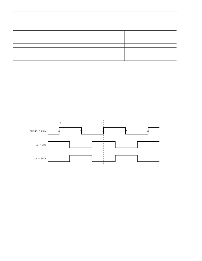
AC Timing Diagrams
20004532
FIGURE 1. “Alternate High/Low” Test Pattern in 12-bit Input Mode
(Note 8)
D
www.national.com
7
相關(guān)PDF資料 |
PDF描述 |
|---|---|
| SLE11C001S-C | 5015 RR 4#12 18#16 SKT RECP |
| SLE11C001S-V5-C | Security & Chip Card ICs |
| SLE11C001S-V5-F7-C | Security & Chip Card ICs |
| SLE11C001S-V5-F7-M4 | Security & Chip Card ICs |
| SLE11C001S-V5-M4 | Security & Chip Card ICs |
相關(guān)代理商/技術(shù)參數(shù) |
參數(shù)描述 |
|---|---|
| SLB1340R45 | 功能描述:滑動開關(guān) Mini Slide Switch RoHS:否 制造商:C&K Components 觸點形式:SPDT 開關(guān)功能:Momentary 觸點額定值: 端接類型: 執(zhí)行器:Extended, Side 安裝風(fēng)格:SMD/SMT 觸點電鍍:Silver 封裝: |
| SLB134145 | 功能描述:滑動開關(guān) Mini Slide Switch RoHS:否 制造商:C&K Components 觸點形式:SPDT 開關(guān)功能:Momentary 觸點額定值: 端接類型: 執(zhí)行器:Extended, Side 安裝風(fēng)格:SMD/SMT 觸點電鍍:Silver 封裝: |
| SLB1370 | 功能描述:滑動開關(guān) MINI SLIDE SWITCH RoHS:否 制造商:C&K Components 觸點形式:SPDT 開關(guān)功能:Momentary 觸點額定值: 端接類型: 執(zhí)行器:Extended, Side 安裝風(fēng)格:SMD/SMT 觸點電鍍:Silver 封裝: |
| SLB1370R | 功能描述:滑動開關(guān) SP3T 0.3A 125V On-On-On RoHS:否 制造商:C&K Components 觸點形式:SPDT 開關(guān)功能:Momentary 觸點額定值: 端接類型: 執(zhí)行器:Extended, Side 安裝風(fēng)格:SMD/SMT 觸點電鍍:Silver 封裝: |
| SLB13804 | 功能描述:滑動開關(guān) SP3T 0.3A 125V On-On-On RoHS:否 制造商:C&K Components 觸點形式:SPDT 開關(guān)功能:Momentary 觸點額定值: 端接類型: 執(zhí)行器:Extended, Side 安裝風(fēng)格:SMD/SMT 觸點電鍍:Silver 封裝: |
發(fā)布緊急采購,3分鐘左右您將得到回復(fù)。