- 您現(xiàn)在的位置:買賣IC網(wǎng) > PDF目錄373626 > TDA9109N (意法半導(dǎo)體) LOW-COST DEFLECTION PROCESSOR FOR MULTISYNC MONITORS PDF資料下載
參數(shù)資料
| 型號: | TDA9109N |
| 廠商: | 意法半導(dǎo)體 |
| 英文描述: | LOW-COST DEFLECTION PROCESSOR FOR MULTISYNC MONITORS |
| 中文描述: | 低費(fèi)用偏轉(zhuǎn)處理器多同步監(jiān)測儀 |
| 文件頁數(shù): | 19/32頁 |
| 文件大小: | 303K |
| 代理商: | TDA9109N |
第1頁第2頁第3頁第4頁第5頁第6頁第7頁第8頁第9頁第10頁第11頁第12頁第13頁第14頁第15頁第16頁第17頁第18頁當(dāng)前第19頁第20頁第21頁第22頁第23頁第24頁第25頁第26頁第27頁第28頁第29頁第30頁第31頁第32頁
OPERATINGDESCRIPTION
(continued)
Thesyncfrequencymustalwaysbe higherthanthe
freerunningfrequency.For example,whenusinga
sync range between 24kHz and 100kHz, the sug-
gestedfreerunning frequencyis 23kHz.
This can be obtained only by adjusting f
0
(for in-
stance, makingR
0
adjustable).If no adjustment is
possible, more margin must be provided to cope
withthe componentsspread :
±
8% for the IC,
±
1%
forR
0
,
±
2 or5%for C
0
, leadingto
±
11%or 14%on
f
0
. The same percentage of frequency range will
lostat upperend of the range.
Another feature is the capability for the MCU to
force the horizontal frequencythrough I
2
C to 2xf0
or 3xf0 (for burn-in mode or safety requirements).
Inthiscase,theinhibitionswitchisopened,leaving
PLL1 free, but the voltage on PLL1 filter is forced
to 2.66V (for 2xf0) or 4.0V (for 3xf0).
PLL1ensuresthecoincidencebetweentheleading
edge of the sync signal and a phase reference
obtained by comparison between the sawtooth of
the VCO and an internal DC voltage which is I
2
C
adjustablebetween 2.8Vand 4.0V(corresponding
to
±
10%)(seeFigure 10).
TheTDA9109/Nalsoincludesa Lock/Unlockiden-
tification block which senses in real time whether
PLL1 is locked or not on the incoming horizontal
sync signal. The resulting information is available
on HLOCKOUT(see Sync Processor).
When PLL1 is unlocked, it forces HLOCKOUT to
high level.
The lock/unlock information is also available
throughthe I
2
C read.
H Osc
Sawtooth
Phase REF1
H Synchro
1.6V
Vb
6.4V
2.8V < Vb < 4.0V
7/8T
H
1/8T
H
Phase REF1is obtainedbycomparisonbetweenthesawtoothand
a DC voltage adjustable between 2.8V and 4.0V. The PLL1 en-
sures the exact coincidence between the signal phase REF and
HSYNC. A
±
T
H
/10 phase adjustment is possible.
9
Figure 10 :
PLL1Timing Diagram
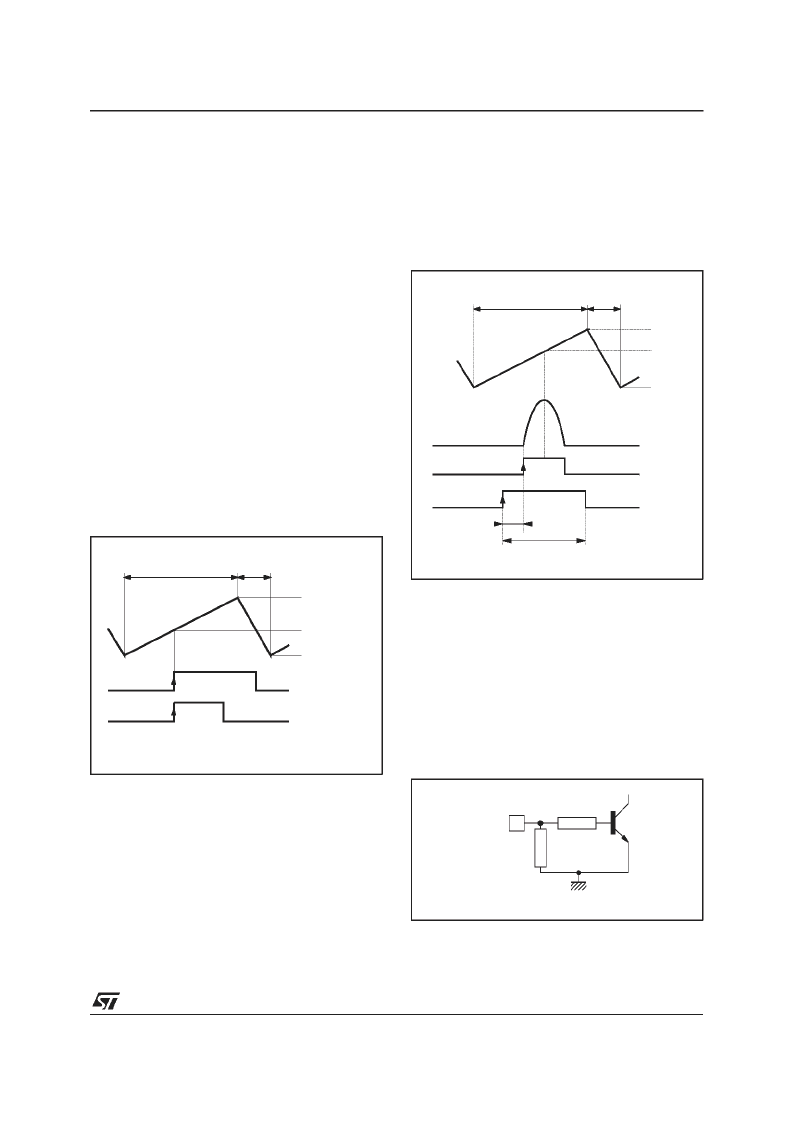
II.3 - PLL2
PLL2 ensures a constant position of the shaped
flyback signal in comparison with the sawtooth of
theVCO, takinginto accountthe saturationtimeTs
(seeFigure 11).
H Osc
Sawtooth
H Drive
1.6V
4.0V
6.4V
7/8T
H
1/8T
H
Ts
Duty Cycle
Internally
Shaped Flyback
Flyback
The duty cycle of H-drive is fixed (48%).
9
Figure 11:
PLL2Timing Diagram
The phase comparator of PLL2 (phase type com-
parator) is followed by a charge pump (typical
outputcurrent: 0.5mA).
The flyback input consists of an NPN transistor.
This input must be current driven. The maximum
recommendedinputcurrentis 5mA(seeFigure12).
The duty cycle is fixed (48%).
The maximum storage time (Ts Max.) is (0.44T
H
-
T
FLY
/2). Typically, T
FLY
/T
H
is around 20% which
means that Ts max is around 34% of T
H
.
20k
Q1
GND 0V
12
HFLY
400
9
Figure 12 :
Flyback Input Electrical Diagram
TDA9109/N
19/32
相關(guān)PDF資料 |
PDF描述 |
|---|---|
| TDA9109SN | LOW-COST DEFLECTION PROCESSOR FOR MULTISYNC MONITORS |
| TDA9109 | LOW-COST DEFLECTION PROCESSOR FOR MULTISYNC MONITORS |
| TDA9109S | LOW-COST DEFLECTION PROCESSOR FOR MULTISYNC MONITORS |
| TDA9110 | LOW-COST DEFLECTION PROCESSOR FOR MULTISYNC MONITORS |
| TDA9111 | LOW-COST I2C CONTROLLED DEFLECTION PROCESSOR FOR MULTISYNC MONITOR |
相關(guān)代理商/技術(shù)參數(shù) |
參數(shù)描述 |
|---|---|
| TDA9109S | 制造商:STMICROELECTRONICS 制造商全稱:STMicroelectronics 功能描述:LOW-COST DEFLECTION PROCESSOR FOR MULTISYNC MONITORS |
| TDA9109SN | 制造商:STMICROELECTRONICS 制造商全稱:STMicroelectronics 功能描述:LOW-COST DEFLECTION PROCESSOR FOR MULTISYNC MONITORS |
| TDA9110 | 制造商:STMicroelectronics 功能描述:TDA9110 - Bulk |
| TDA9111 | 制造商:STMICROELECTRONICS 制造商全稱:STMicroelectronics 功能描述:LOW-COST I2C CONTROLLED DEFLECTION PROCESSOR FOR MULTISYNC MONITOR |
| TDA9112 | 制造商:STMICROELECTRONICS 制造商全稱:STMicroelectronics 功能描述:LOW-COST I2C CONTROLLED DEFLECTION PROCESSOR FOR MULTISYNC MONITOR |
發(fā)布緊急采購,3分鐘左右您將得到回復(fù)。