- 您現(xiàn)在的位置:買賣IC網(wǎng) > PDF目錄383961 > TMX320DM6437BZDUA (Texas Instruments, Inc.) Digital Media Processor PDF資料下載
參數(shù)資料
| 型號: | TMX320DM6437BZDUA |
| 廠商: | Texas Instruments, Inc. |
| 英文描述: | Digital Media Processor |
| 中文描述: | 數(shù)字媒體處理器 |
| 文件頁數(shù): | 213/309頁 |
| 文件大小: | 2216K |
| 代理商: | TMX320DM6437BZDUA |
第1頁第2頁第3頁第4頁第5頁第6頁第7頁第8頁第9頁第10頁第11頁第12頁第13頁第14頁第15頁第16頁第17頁第18頁第19頁第20頁第21頁第22頁第23頁第24頁第25頁第26頁第27頁第28頁第29頁第30頁第31頁第32頁第33頁第34頁第35頁第36頁第37頁第38頁第39頁第40頁第41頁第42頁第43頁第44頁第45頁第46頁第47頁第48頁第49頁第50頁第51頁第52頁第53頁第54頁第55頁第56頁第57頁第58頁第59頁第60頁第61頁第62頁第63頁第64頁第65頁第66頁第67頁第68頁第69頁第70頁第71頁第72頁第73頁第74頁第75頁第76頁第77頁第78頁第79頁第80頁第81頁第82頁第83頁第84頁第85頁第86頁第87頁第88頁第89頁第90頁第91頁第92頁第93頁第94頁第95頁第96頁第97頁第98頁第99頁第100頁第101頁第102頁第103頁第104頁第105頁第106頁第107頁第108頁第109頁第110頁第111頁第112頁第113頁第114頁第115頁第116頁第117頁第118頁第119頁第120頁第121頁第122頁第123頁第124頁第125頁第126頁第127頁第128頁第129頁第130頁第131頁第132頁第133頁第134頁第135頁第136頁第137頁第138頁第139頁第140頁第141頁第142頁第143頁第144頁第145頁第146頁第147頁第148頁第149頁第150頁第151頁第152頁第153頁第154頁第155頁第156頁第157頁第158頁第159頁第160頁第161頁第162頁第163頁第164頁第165頁第166頁第167頁第168頁第169頁第170頁第171頁第172頁第173頁第174頁第175頁第176頁第177頁第178頁第179頁第180頁第181頁第182頁第183頁第184頁第185頁第186頁第187頁第188頁第189頁第190頁第191頁第192頁第193頁第194頁第195頁第196頁第197頁第198頁第199頁第200頁第201頁第202頁第203頁第204頁第205頁第206頁第207頁第208頁第209頁第210頁第211頁第212頁當前第213頁第214頁第215頁第216頁第217頁第218頁第219頁第220頁第221頁第222頁第223頁第224頁第225頁第226頁第227頁第228頁第229頁第230頁第231頁第232頁第233頁第234頁第235頁第236頁第237頁第238頁第239頁第240頁第241頁第242頁第243頁第244頁第245頁第246頁第247頁第248頁第249頁第250頁第251頁第252頁第253頁第254頁第255頁第256頁第257頁第258頁第259頁第260頁第261頁第262頁第263頁第264頁第265頁第266頁第267頁第268頁第269頁第270頁第271頁第272頁第273頁第274頁第275頁第276頁第277頁第278頁第279頁第280頁第281頁第282頁第283頁第284頁第285頁第286頁第287頁第288頁第289頁第290頁第291頁第292頁第293頁第294頁第295頁第296頁第297頁第298頁第299頁第300頁第301頁第302頁第303頁第304頁第305頁第306頁第307頁第308頁第309頁
www.ti.com
P
6.9.4
DDR2 Memory Controller
TMS320DM6437
Digital Media Processor
SPRS345B–NOVEMBER 2006–REVISED MARCH 2007
The DDR2 Memory Controller is a dedicated interface to DDR2 SDRAM. It supports JESD79D-2A
standard compliant DDR2 SDRAM Devices and can interface to either 16-bit or 32-bit DDR2 SDRAM
devices. For details on the DDR2 Memory Controller, see the
TMS320DM643x DMP DDR2 Memory
Controller
User’s Guide (literature number
SPRU986
).
DDR2 SDRAM plays a key role in a DaVinci-based system. Such a system is expected to require a
significant amount of high-speed external memory for:
Buffering of input image data from sensors or video sources
Intermediate buffering for processing/resizing of image data in the VPFE
Numerous OSD display buffers
Intermediate buffering for large raw Bayer data image files while performing image processing
functions
Buffering for intermediate data while performing video encode and decode functions
Storage of executable code for the DSP
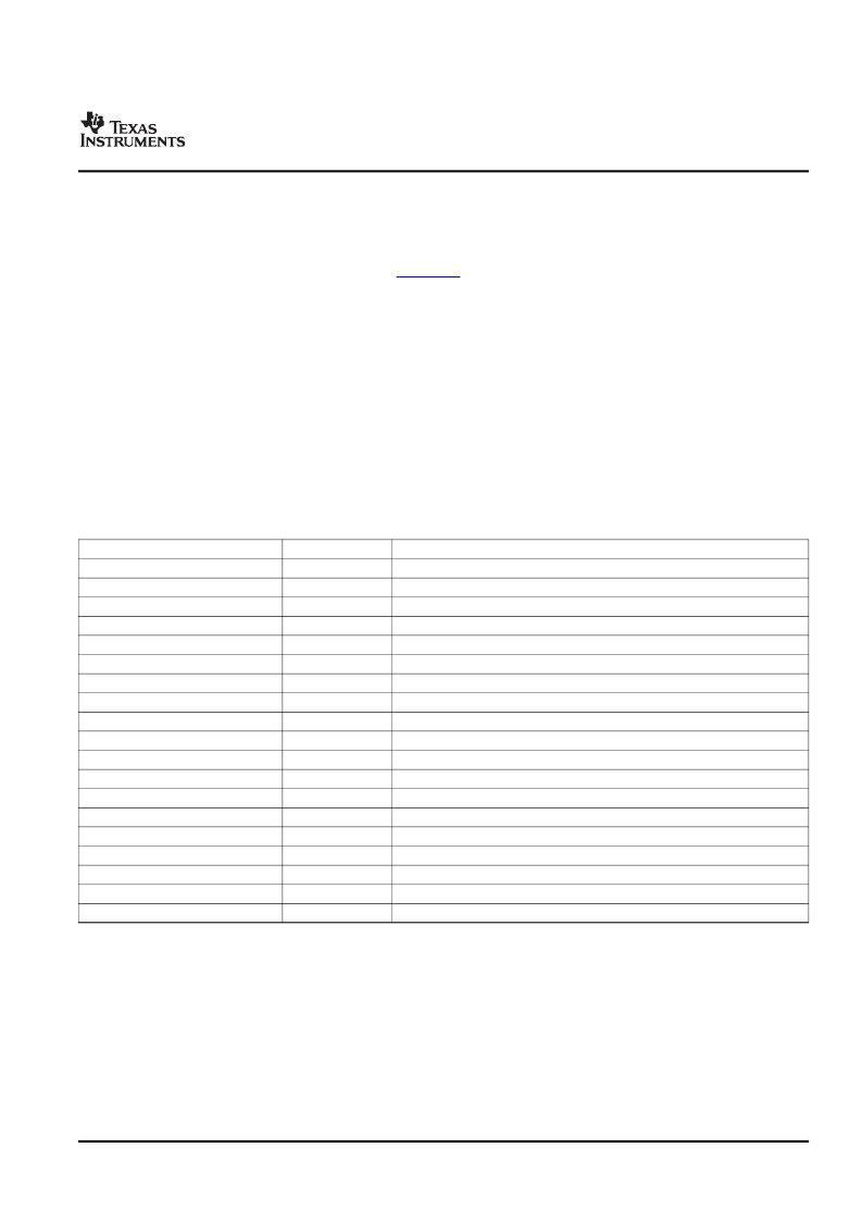
A memory map of the DDR2 Memory Controller registers is shown in
Table 6-26
.
Table 6-26. DDR2 Memory Controller Registers
HEX ADDRESS RANGE
0x01C4 004C
0x01C4 2038
0x2000 0000 - 0x2000 0003
0x2000 0004
0x2000 0008
0x2000 000C
0x2000 0010
0x2000 0014
0x2000 0020
0x2000 0024 - 0x2000 00BF
0x2000 00C0
0x2000 00C4
0x2000 00C8
0x2000 00CC
0x2000 00D0 - 0x2000 00E3
0x2000 00E4
0x2000 00E8 - 0x2000 00EF
0x2000 00F0
0x2000 00F4 - 0x2000 7FFF
ACRONYM
DDRVTPER
DDRVTPR
-
SDRSTAT
SDBCR
SDRCR
SDTIMR
SDTIMR2
PBBPR
-
IRR
IMR
IMSR
IMCR
-
DDRPHYCR
-
VTPIOCR
-
REGISTER NAME
DDR2 VTP Enable Register
DDR2 VTP Register
Reserved
SDRAM Status Register
SDRAM Bank Configuration Register
SDRAM Refresh Control Register
SDRAM Timing Register
SDRAM Timing Register 2
Peripheral Bus Burst Priority Register
Reserved
Interrupt Raw Register
Interrupt Masked Register
Interrupt Mask Set Register
Interrupt Mask Clear Register
Reserved
DDR PHY Control Register
Reserved
DDR VTP IO Control Register
Reserved
6.9.4.1
DDR2 Memory Controller Electrical Data/Timing
The
Implementing DDR2 PCB Layout on the DM643x Digital Media Processor
application report (literature
number TBD) specifies a complete DDR2 interface solution for the DM6437 as well as a list of compatible
DDR2 devices. TI has performed the simulation and system characterization to ensure all DDR2 interface
timings in this solution are met.
TI only supports board designs that follow the guidelines outlined in the
Implementing DDR2 PCB Layout
on the DM643x Digital Media Processor
application report (literature number TBD ulink).
Submit Documentation Feedback
Peripheral Information and Electrical Specifications
213
相關PDF資料 |
PDF描述 |
|---|---|
| TMX320DM6437BZWTA | Digital Media Processor |
| TMS320DM6443_07 | Digital Media System-on-Chip |
| TMX320DM6443AZWT | Digital Media System-on-Chip |
| TMX320DM6443ZWT | Digital Media System-on-Chip |
| TMS320DM647_08 | Digital Media Processor |
相關代理商/技術參數(shù) |
參數(shù)描述 |
|---|---|
| TMX320DM6437BZWTA | 功能描述:數(shù)字信號處理器和控制器 - DSP, DSC Dig Media Processor RoHS:否 制造商:Microchip Technology 核心:dsPIC 數(shù)據(jù)總線寬度:16 bit 程序存儲器大小:16 KB 數(shù)據(jù) RAM 大小:2 KB 最大時鐘頻率:40 MHz 可編程輸入/輸出端數(shù)量:35 定時器數(shù)量:3 設備每秒兆指令數(shù):50 MIPs 工作電源電壓:3.3 V 最大工作溫度:+ 85 C 封裝 / 箱體:TQFP-44 安裝風格:SMD/SMT |
| TMX320DM6441CZWT | 制造商:Texas Instruments 功能描述: |
| TMX320DM6441DZWT | 制造商:Texas Instruments 功能描述:DAVINCI DIGITAL MEDIA SYSTEM-ON-CHIP - Tape and Reel |
| TMX320DM6443AZWT | 制造商:Rochester Electronics LLC 功能描述:DAVINCI DIGITAL MEDIA SYSTEM-ON-CHIP - Tape and Reel |
| TMX320DM6443BZWT | 制造商:Texas Instruments 功能描述: |
發(fā)布緊急采購,3分鐘左右您將得到回復。