- 您現(xiàn)在的位置:買賣IC網 > PDF目錄384024 > TMX320DM6446ZWT (Texas Instruments, Inc.) Digital Media System on-Chip PDF資料下載
參數(shù)資料
| 型號: | TMX320DM6446ZWT |
| 廠商: | Texas Instruments, Inc. |
| 英文描述: | Digital Media System on-Chip |
| 中文描述: | 數(shù)字媒體系統(tǒng)芯片 |
| 文件頁數(shù): | 31/214頁 |
| 文件大小: | 1699K |
| 代理商: | TMX320DM6446ZWT |
第1頁第2頁第3頁第4頁第5頁第6頁第7頁第8頁第9頁第10頁第11頁第12頁第13頁第14頁第15頁第16頁第17頁第18頁第19頁第20頁第21頁第22頁第23頁第24頁第25頁第26頁第27頁第28頁第29頁第30頁當前第31頁第32頁第33頁第34頁第35頁第36頁第37頁第38頁第39頁第40頁第41頁第42頁第43頁第44頁第45頁第46頁第47頁第48頁第49頁第50頁第51頁第52頁第53頁第54頁第55頁第56頁第57頁第58頁第59頁第60頁第61頁第62頁第63頁第64頁第65頁第66頁第67頁第68頁第69頁第70頁第71頁第72頁第73頁第74頁第75頁第76頁第77頁第78頁第79頁第80頁第81頁第82頁第83頁第84頁第85頁第86頁第87頁第88頁第89頁第90頁第91頁第92頁第93頁第94頁第95頁第96頁第97頁第98頁第99頁第100頁第101頁第102頁第103頁第104頁第105頁第106頁第107頁第108頁第109頁第110頁第111頁第112頁第113頁第114頁第115頁第116頁第117頁第118頁第119頁第120頁第121頁第122頁第123頁第124頁第125頁第126頁第127頁第128頁第129頁第130頁第131頁第132頁第133頁第134頁第135頁第136頁第137頁第138頁第139頁第140頁第141頁第142頁第143頁第144頁第145頁第146頁第147頁第148頁第149頁第150頁第151頁第152頁第153頁第154頁第155頁第156頁第157頁第158頁第159頁第160頁第161頁第162頁第163頁第164頁第165頁第166頁第167頁第168頁第169頁第170頁第171頁第172頁第173頁第174頁第175頁第176頁第177頁第178頁第179頁第180頁第181頁第182頁第183頁第184頁第185頁第186頁第187頁第188頁第189頁第190頁第191頁第192頁第193頁第194頁第195頁第196頁第197頁第198頁第199頁第200頁第201頁第202頁第203頁第204頁第205頁第206頁第207頁第208頁第209頁第210頁第211頁第212頁第213頁第214頁
www.ti.com
P
TMS320DM6446
Digital Media System on-Chip
SPRS283–DECEMBER 2005
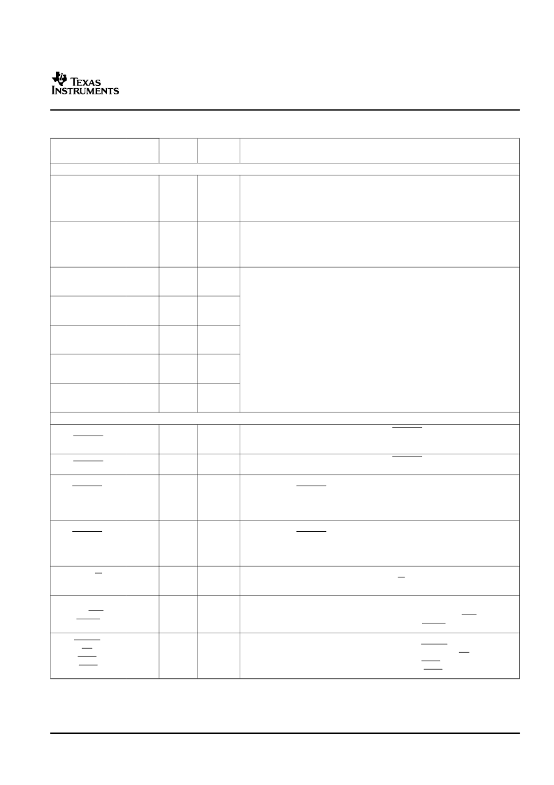
Table 2-13. EMIFA Terminal Functions
SIGNAL
NAME
IPD/
IPU
(2)
TYPE
(1)
DESCRIPTION
NO.
EMIFA BOOT CONFIGURATION
This pin is multiplexed between EMIFA and the VPBE. At reset, the input state is
sampled to set the EMIFA data bus width (EM_WIDTH). For an 8-bit wide EMIFA
data bus, EM_WIDTH = 0. For a 16-bit wide EMIFA data bus, EM_WIDTH = 1.
After reset, it is video encoder output COUT2 or RGB666/888 Blue output data bit
5 B5.
This pin is multiplexed between DSP boot and the VPBE. At reset, the input state
is sampled to set the DSP boot source DSP_BT. The DSP is booted by the ARM
when DSP_BT=0. The DSP boots from EMIFA when DSP_BT=1.
After reset, it is video encoder output COUT3 or RGB666/888 Blue data bit 6
output B6.
COUT2/
B5/
EM_WIDTH
A17
I/O/Z
IPD
COUT3/
B6/
DSP_BT
B17
I/O/Z
IPD
YOUT0/
G5/
AEAW0
YOUT1/
G6/
AEAW1
YOUT2/
G7/
AEAW2
YOUT3/
R3/
AEAW3
YOUT4/
R4/
AEAW4
D15
I/O/Z
IPD
D16
I/O/Z
IPD
These pins are multiplexed between EMIFA and the VPBE. At reset, the input
states of AEAW[4:0] are sampled to set the EMIFA address bus width. See the
Peripheral Selection at Device Reset section for details.
After reset, these are video encoder outputs YOUT[0:4] or RGB666/888 Red and
Green data bit outputs G5, G6, G7, R3, and R4.
D17
I/O/Z
IPD
D18
I/O/Z
IPD
E15
I/O/Z
IPD
EMIFA FUNCTIONAL PINS: ASYNC / NOR
For EMIFA, this pin is Chip Select 2 output EM_CS2 for use with asynchronous
IPD
memories (i.e., NOR flash) or NAND flash. This is the chip select for the default
boot and ROM boot modes.
For EMIFA, this pin is Chip Select 3 output EM_CS3 for use with asynchronous
IPD
memories (i.e., NOR flash) or NAND flash.
This pin is multiplexed between EMIFA, GPIO, and VLYNQ. For EMIFA, it is Chip
Select 4 output EM_CS4 for use with asynchronous memories (i.e., NOR flash) or
IPD
NAND flash.
For GPIO, it is GPIO9.
For VLYNQ, it is the Serial Clock run request VLYNQ_SCRUN.
This pin is multiplexed between EMIFA, GPIO, and VLYNQ. For EMIFA, it is Chip
Select 5 output EM_CS5 for use with asynchronous memories (i.e., NOR flash) or
IPD
NAND flash.
For GPIO, it is GPIO pin 8 GPIO8
For VLYNQ, it is the clock VLYNQ_CLOCK.
This pin is multiplexed between EMIFA and ATA/CF. For EMIFA, it is read/write
IPD
output EM_R/W.
For ATA/CF, it is interrupt request input INTRQ.
This pin is multiplexed between EMIFA (NAND/SmartMedia/xD) and ATA/CF. For
EMIFA, it is wait state extension input EM_WAIT.
IPD
For NAND/SmartMedia/xD, it is ready/busy input (RDY/BSY).
For ATA/CF, it is IO Ready input IORDY.
This pin is multiplexed between EMIFA (NAND/SmartMedia/xD) and ATA/CF. For
EMIFA, it is output enable output EM_OE.
IPD
For NAND/SmartMedia/xD, it is read enable output (RE).
For CF, it is read strobe output (IORD).
For ATA, it is read strobe output DIOR.
EM_CS2
C2
I/O/Z
EM_CS3
B1
I/O/Z
EM_CS4/
GPIO9/
VLYNQ_SCRUN
T2
I/O/Z
EM_CS5/
GPIO8/
VLYNQ_CLOCK
T1
I/O/Z
EM_R/W/
INTRQ
G3
I/O/Z
EM_WAIT/
(RDY/BSY)/
IORDY
F1
I/O/Z
EM_OE/
(RE)/
(IORD)/
DIOR
H4
I/O/Z
(1)
(2)
I = Input, O = Output, Z = High impedance, S = Supply voltage, GND = Ground, A = Analog signal
IPD = Internal pulldown, IPU = Internal pullup. (To pull up a signal to the opposite supply rail, a 1-k
resistor should be used.)
Device Overview
31
相關PDF資料 |
PDF描述 |
|---|---|
| TN28F010-90 | 28F010 1024K (128K X 8) CMOS FLASH MEMORY |
| TN28F010-120 | 28F010 1024K (128K X 8) CMOS FLASH MEMORY |
| TN28F010-150 | 28F010 1024K (128K X 8) CMOS FLASH MEMORY |
| TN28F020-90 | 28F020 2048K (256K X 8) CMOS FLASH MEMORY |
| TN28F020-150 | 28F020 2048K (256K X 8) CMOS FLASH MEMORY |
相關代理商/技術參數(shù) |
參數(shù)描述 |
|---|---|
| TMX320DM6467TZUT1 | 制造商:Texas Instruments 功能描述: |
| TMX320DM6467ZUT | 功能描述:數(shù)字信號處理器和控制器 - DSP, DSC Dig Media System-on- Chip RoHS:否 制造商:Microchip Technology 核心:dsPIC 數(shù)據總線寬度:16 bit 程序存儲器大小:16 KB 數(shù)據 RAM 大小:2 KB 最大時鐘頻率:40 MHz 可編程輸入/輸出端數(shù)量:35 定時器數(shù)量:3 設備每秒兆指令數(shù):50 MIPs 工作電源電壓:3.3 V 最大工作溫度:+ 85 C 封裝 / 箱體:TQFP-44 安裝風格:SMD/SMT |
| TMX320DM647ZUT720 | 制造商:TI 制造商全稱:Texas Instruments 功能描述:Digital Media Processor |
| TMX320DM647ZUT900 | 制造商:TI 制造商全稱:Texas Instruments 功能描述:Digital Media Processor |
| TMX320DM648ACUT7 | 制造商:Texas Instruments 功能描述:- Trays |
發(fā)布緊急采購,3分鐘左右您將得到回復。