- 您現(xiàn)在的位置:買(mǎi)賣(mài)IC網(wǎng) > PDF目錄384024 > TMX320DM6446ZWT (Texas Instruments, Inc.) Digital Media System on-Chip PDF資料下載
參數(shù)資料
| 型號(hào): | TMX320DM6446ZWT |
| 廠(chǎng)商: | Texas Instruments, Inc. |
| 英文描述: | Digital Media System on-Chip |
| 中文描述: | 數(shù)字媒體系統(tǒng)芯片 |
| 文件頁(yè)數(shù): | 84/214頁(yè) |
| 文件大小: | 1699K |
| 代理商: | TMX320DM6446ZWT |
第1頁(yè)第2頁(yè)第3頁(yè)第4頁(yè)第5頁(yè)第6頁(yè)第7頁(yè)第8頁(yè)第9頁(yè)第10頁(yè)第11頁(yè)第12頁(yè)第13頁(yè)第14頁(yè)第15頁(yè)第16頁(yè)第17頁(yè)第18頁(yè)第19頁(yè)第20頁(yè)第21頁(yè)第22頁(yè)第23頁(yè)第24頁(yè)第25頁(yè)第26頁(yè)第27頁(yè)第28頁(yè)第29頁(yè)第30頁(yè)第31頁(yè)第32頁(yè)第33頁(yè)第34頁(yè)第35頁(yè)第36頁(yè)第37頁(yè)第38頁(yè)第39頁(yè)第40頁(yè)第41頁(yè)第42頁(yè)第43頁(yè)第44頁(yè)第45頁(yè)第46頁(yè)第47頁(yè)第48頁(yè)第49頁(yè)第50頁(yè)第51頁(yè)第52頁(yè)第53頁(yè)第54頁(yè)第55頁(yè)第56頁(yè)第57頁(yè)第58頁(yè)第59頁(yè)第60頁(yè)第61頁(yè)第62頁(yè)第63頁(yè)第64頁(yè)第65頁(yè)第66頁(yè)第67頁(yè)第68頁(yè)第69頁(yè)第70頁(yè)第71頁(yè)第72頁(yè)第73頁(yè)第74頁(yè)第75頁(yè)第76頁(yè)第77頁(yè)第78頁(yè)第79頁(yè)第80頁(yè)第81頁(yè)第82頁(yè)第83頁(yè)當(dāng)前第84頁(yè)第85頁(yè)第86頁(yè)第87頁(yè)第88頁(yè)第89頁(yè)第90頁(yè)第91頁(yè)第92頁(yè)第93頁(yè)第94頁(yè)第95頁(yè)第96頁(yè)第97頁(yè)第98頁(yè)第99頁(yè)第100頁(yè)第101頁(yè)第102頁(yè)第103頁(yè)第104頁(yè)第105頁(yè)第106頁(yè)第107頁(yè)第108頁(yè)第109頁(yè)第110頁(yè)第111頁(yè)第112頁(yè)第113頁(yè)第114頁(yè)第115頁(yè)第116頁(yè)第117頁(yè)第118頁(yè)第119頁(yè)第120頁(yè)第121頁(yè)第122頁(yè)第123頁(yè)第124頁(yè)第125頁(yè)第126頁(yè)第127頁(yè)第128頁(yè)第129頁(yè)第130頁(yè)第131頁(yè)第132頁(yè)第133頁(yè)第134頁(yè)第135頁(yè)第136頁(yè)第137頁(yè)第138頁(yè)第139頁(yè)第140頁(yè)第141頁(yè)第142頁(yè)第143頁(yè)第144頁(yè)第145頁(yè)第146頁(yè)第147頁(yè)第148頁(yè)第149頁(yè)第150頁(yè)第151頁(yè)第152頁(yè)第153頁(yè)第154頁(yè)第155頁(yè)第156頁(yè)第157頁(yè)第158頁(yè)第159頁(yè)第160頁(yè)第161頁(yè)第162頁(yè)第163頁(yè)第164頁(yè)第165頁(yè)第166頁(yè)第167頁(yè)第168頁(yè)第169頁(yè)第170頁(yè)第171頁(yè)第172頁(yè)第173頁(yè)第174頁(yè)第175頁(yè)第176頁(yè)第177頁(yè)第178頁(yè)第179頁(yè)第180頁(yè)第181頁(yè)第182頁(yè)第183頁(yè)第184頁(yè)第185頁(yè)第186頁(yè)第187頁(yè)第188頁(yè)第189頁(yè)第190頁(yè)第191頁(yè)第192頁(yè)第193頁(yè)第194頁(yè)第195頁(yè)第196頁(yè)第197頁(yè)第198頁(yè)第199頁(yè)第200頁(yè)第201頁(yè)第202頁(yè)第203頁(yè)第204頁(yè)第205頁(yè)第206頁(yè)第207頁(yè)第208頁(yè)第209頁(yè)第210頁(yè)第211頁(yè)第212頁(yè)第213頁(yè)第214頁(yè)
www.ti.com
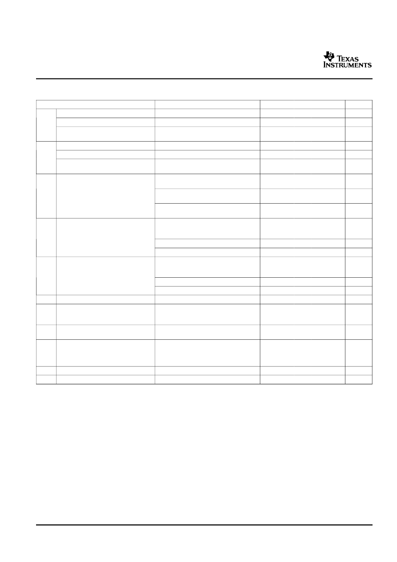
P
4.3
Electrical Characteristics Over Recommended Ranges of Supply Voltage and Operating
Case Temperature (Unless Otherwise Noted)
PARAMETER
TEST CONDITIONS
(1)
High-level output voltage (3.3V I/O)
DV
DD33
= MIN, I
OH
= MAX
High-level output voltage (1.8V I/O)
DV
DD18
= MIN, I
OH
= MAX
High-level output voltage (1.8V I/O
DV
DDR
= MIN, I
OH
= MAX
DDR2)
Low-level output voltage (3.3V I/O)
DV
DD33
= MIN, I
OL
= MAX
Low-level output voltage (1.8V I/O)
DV
DD18
= MIN, I
OL
= MAX
Low-level output voltage (1.8V I/O
DV
DDR
= MIN, I
OL
= MAX
DDR2)
V
= V
to DV
DD
without opposing
internal resistor
V
= V
to DV
(2)
with opposing internal
Input current
pullup resistor
V
= V
to DV
with opposing internal
pulldown resistor
(2)
VCLK, GPIO[48]/CLK_OUT0,
GPIO[8]/EM_CS5/VLYNQ_CLK,
EM_A[21:14]/VLYNQ_(TX/RX)D[3:0]
High-level output current
DDR2
All other peripherals
VCLK, GPIO[48]/CLK_OUT0,
GPIO[8]/EM_CS5/VLYNQ_CLK,
EM_A[21:14]/VLYNQ_(TX/RX)D[3:0]
Low-level output current
DDR2
All other peripherals
I/O Off-state output current
V
O
= DV
DD
or V
SS
Core (CV
, APLLREFV, V
,
V
DDA1P2LDD
, CV
DDDSP
) supply
CV
DD
= 1.2 V, DSP clock = 594 MHz
current
(4)
3.3V I/O (DV
D(4)
, USB_DV
DDA3P3
)
DV
DD
= 3.3 V, DSP clock = 594 MHz
supply current
1.8V I/O (DV
DD18
, DV
DDR2
,
DDR_V
DDDLL
,
DV
DD
= 1.8 V, DSP clock = 594 MHz
USB_V
, MXVDD, M24VDD)
supply current
(4)
Input capacitance
Output capacitance
TMS320DM6446
Digital Media System on-Chip
SPRS283–DECEMBER 2005
MIN
TYP
MAX
UNIT
V
V
DV
DD
- 0.2
DV
DD
- 0.45
DDR_VREF
+ 0.643
V
OH
V
0.2
0.45
V
V
V
OL
DDR_VREF
- 0.643
V
1
μA
I
I
TBD
μA
TBD
μA
8
mA
I
OH
-13.4
mA
mA
4
8
mA
I
OL
13.4
mA
mA
μA
4
I
OZ
±
20
I
CDD
TBD
mA
I
DDD
TBD
mA
I
DDD
TBD
mA
C
i
C
o
10
10
pF
pF
(1)
(2)
(3)
(4)
For test conditions shown as MIN, MAX, or NOM, use the appropriate value specified in the recommended operating conditions table.
Applies only to pins with an internal pullup (IPU) or pulldown (IPD) resistor.
This pin is an internal LDO output and connected via 1 μF capacitor to USB_V
.
Measured with average activity (50% high/50% low power) at 25
°
C case temperature and TBD-MHz EMIFA for -594 speed. This model
represents a device performing high-MPU/DSP-activity operations 50% of the time, and the remainder performing low-MPU/DSP-activity
operations. The high/low-MPU/DSP-activity models are defined as follows:
High-MPU/DSP-Activity Model:
–
MPU: TBD
–
DSP: TBD
Low-MPU/DSP-Activity Model:
–
MPU: TBD
–
DSP: TBD
The actual current draw is highly application-dependent. For more details on core and I/O activity, see the
DM644xPower Consumption
Summary
application report (literature number SPRATBD).
84
Device Operating Conditions
相關(guān)PDF資料 |
PDF描述 |
|---|---|
| TN28F010-90 | 28F010 1024K (128K X 8) CMOS FLASH MEMORY |
| TN28F010-120 | 28F010 1024K (128K X 8) CMOS FLASH MEMORY |
| TN28F010-150 | 28F010 1024K (128K X 8) CMOS FLASH MEMORY |
| TN28F020-90 | 28F020 2048K (256K X 8) CMOS FLASH MEMORY |
| TN28F020-150 | 28F020 2048K (256K X 8) CMOS FLASH MEMORY |
相關(guān)代理商/技術(shù)參數(shù) |
參數(shù)描述 |
|---|---|
| TMX320DM6467TZUT1 | 制造商:Texas Instruments 功能描述: |
| TMX320DM6467ZUT | 功能描述:數(shù)字信號(hào)處理器和控制器 - DSP, DSC Dig Media System-on- Chip RoHS:否 制造商:Microchip Technology 核心:dsPIC 數(shù)據(jù)總線(xiàn)寬度:16 bit 程序存儲(chǔ)器大小:16 KB 數(shù)據(jù) RAM 大小:2 KB 最大時(shí)鐘頻率:40 MHz 可編程輸入/輸出端數(shù)量:35 定時(shí)器數(shù)量:3 設(shè)備每秒兆指令數(shù):50 MIPs 工作電源電壓:3.3 V 最大工作溫度:+ 85 C 封裝 / 箱體:TQFP-44 安裝風(fēng)格:SMD/SMT |
| TMX320DM647ZUT720 | 制造商:TI 制造商全稱(chēng):Texas Instruments 功能描述:Digital Media Processor |
| TMX320DM647ZUT900 | 制造商:TI 制造商全稱(chēng):Texas Instruments 功能描述:Digital Media Processor |
| TMX320DM648ACUT7 | 制造商:Texas Instruments 功能描述:- Trays |
發(fā)布緊急采購(gòu),3分鐘左右您將得到回復(fù)。