- 您現(xiàn)在的位置:買賣IC網(wǎng) > PDF目錄384024 > TMX320DM6446ZWT (Texas Instruments, Inc.) Digital Media System on-Chip PDF資料下載
參數(shù)資料
| 型號: | TMX320DM6446ZWT |
| 廠商: | Texas Instruments, Inc. |
| 英文描述: | Digital Media System on-Chip |
| 中文描述: | 數(shù)字媒體系統(tǒng)芯片 |
| 文件頁數(shù): | 75/214頁 |
| 文件大小: | 1699K |
| 代理商: | TMX320DM6446ZWT |
第1頁第2頁第3頁第4頁第5頁第6頁第7頁第8頁第9頁第10頁第11頁第12頁第13頁第14頁第15頁第16頁第17頁第18頁第19頁第20頁第21頁第22頁第23頁第24頁第25頁第26頁第27頁第28頁第29頁第30頁第31頁第32頁第33頁第34頁第35頁第36頁第37頁第38頁第39頁第40頁第41頁第42頁第43頁第44頁第45頁第46頁第47頁第48頁第49頁第50頁第51頁第52頁第53頁第54頁第55頁第56頁第57頁第58頁第59頁第60頁第61頁第62頁第63頁第64頁第65頁第66頁第67頁第68頁第69頁第70頁第71頁第72頁第73頁第74頁當前第75頁第76頁第77頁第78頁第79頁第80頁第81頁第82頁第83頁第84頁第85頁第86頁第87頁第88頁第89頁第90頁第91頁第92頁第93頁第94頁第95頁第96頁第97頁第98頁第99頁第100頁第101頁第102頁第103頁第104頁第105頁第106頁第107頁第108頁第109頁第110頁第111頁第112頁第113頁第114頁第115頁第116頁第117頁第118頁第119頁第120頁第121頁第122頁第123頁第124頁第125頁第126頁第127頁第128頁第129頁第130頁第131頁第132頁第133頁第134頁第135頁第136頁第137頁第138頁第139頁第140頁第141頁第142頁第143頁第144頁第145頁第146頁第147頁第148頁第149頁第150頁第151頁第152頁第153頁第154頁第155頁第156頁第157頁第158頁第159頁第160頁第161頁第162頁第163頁第164頁第165頁第166頁第167頁第168頁第169頁第170頁第171頁第172頁第173頁第174頁第175頁第176頁第177頁第178頁第179頁第180頁第181頁第182頁第183頁第184頁第185頁第186頁第187頁第188頁第189頁第190頁第191頁第192頁第193頁第194頁第195頁第196頁第197頁第198頁第199頁第200頁第201頁第202頁第203頁第204頁第205頁第206頁第207頁第208頁第209頁第210頁第211頁第212頁第213頁第214頁
www.ti.com
P
TMS320DM6446
Digital Media System on-Chip
SPRS283–DECEMBER 2005
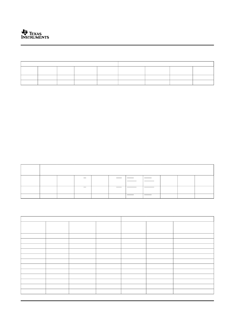
Table 3-23. VPBE (RGB666, RGB888, and LCD) and GPIO Pin Multiplexing
PINMUX0 AND PINMUX1 REGISTER BIT FIELDS
MULTIPLEXED PINS
R1/
GPIO[38]
GPIO[38]
R1
B1/
GPIO[6]
GPIO[6]
B1
G1/
GPIO[5]
GPIO[5]
G1
G0/
GPIO[2]
GPIO[2]
G0
RGB888
PWM2
PWM1
CFLDEN
LFLDEN
0
1
0
0
0
0
0
0
0
0
3.6.6.4
ATA, EMIFA, UART1, SPI, and GPIO Pin Multiplexing
The ATA peripheral shares pins with the EMIFA and UART1 as seen in
Table 3-24
. If ATA pin
functionality is enabled by setting the ATAEN bit field, the ATA module will drive the EMIFA data and
control pins. Enabling UART1 disables the use of the ATA DMARQ and DMACK signals and thus only
allows the ATA module to use PIO mode. The ATA HDDIR buffer direction control bit field works in
conjunction with the HDIREN enable bit field to allow the ATA pins to still be used as a GPIO or SPI_EN1
if the buffer is not being used (i.e. for Compact Flash). This multiplexing is shown in
Table 3-25
. When
ATAEN=0 and HDIREN=1 it indicates that the ATA interface has been disabled so that the EMIFA can be
used, but the ATA buffers are still present. HDDIR is driven low in this situation to ensure that the ATA
buffers drive away from DM644X and don’t cause bus contention with the EMIFA. Note that switching
between EMIFA and ATA (clearing or setting ATAEN) must be carefully performed to prevent bus
contention. Since the ATA device can be a bus master, software must ensure that all outstanding DMA
requests have completed before clearing the ATAEN bit.
Table 3-24. ATA, EMIFA, and GPIO Pin Multiplexing Control
PINMUX0
REGISTER
BIT FIELD
MULTIPLEXED PINS
EM_BA[1]/
GPIO[52]/
ATA1
EM_A[0]/
GPIO[53]/
ATA2
EM_D[15:0]/
DD[15:0]
GPIO[50]/
ATA_CS0
GPIO[51]/
ATA_CS1
EM_R/W
INTRQ
EM_BA[0]/
ATA0
RDY/BSY/
EM_WAIT
DIOR/
EM_OE
DIOW/
EM_WE
ATAEN
GPIO[50]
GPIO[51]
EM_R/W
EM_BA[0]
RDY/BSY
EM_OE
EM_WE
EM_BA[1]/
GPIO[52]
(1)
EM_A[0]/
GPIO[53]
(1)
EM_D[15:0]
0
1
ATA_CS0
ATA_CS1
INTRQ
ATA0
EM_WAIT
DIOR
DIOW
ATA1
ATA2
DD[15:0]
(1)
This pin shares GPIO functionality set by AEAW[4:0] as shown in
Table 3-12
.
Table 3-25. ATA, EMIFA, UART1, SPI, and GPIO Pin Multiplexing
PINMUX0 AND PINMUX1 REGISTER BIT FIELDS
MULTIPLEXED PINS
UART_RXD1/
DMARQ
UART_TXD1/
DMACK
SPI_EN1/
HDDIR/
GPIO[42]
GPIO[42]
SPI_EN1
Driven Low
GPIO[42]
SPI_EN1
Driven Low
GPIO[42]x
SPI_EN1x
HDDIR
GPIO[42]x
SPI_EN1x
HDDIR
ATAEN
UART1
HDIREN
SPI
0
0
0
0
0
0
1
1
1
1
1
1
0
0
0
1
1
1
0
0
0
1
1
1
0
0
1
0
0
1
0
0
1
0
0
1
0
1
-
0
1
-
0
1
-
0
1
-
DMACK
DMACK
DMACK
UART_TXD1
UART_TXD1
UART_TXD1
DMACK
DMACK
DMACK
UART_TXD1
UART_TXD1
UART_TXD1
DMARQ
DMARQ
DMARQ
UART_RXD1
UART_RXD1
UART_RXD1
DMARQ
DMARQ
DMARQ
UART_RXD1
UART_RXD1
UART_RXD1
Device Configuration
75
相關PDF資料 |
PDF描述 |
|---|---|
| TN28F010-90 | 28F010 1024K (128K X 8) CMOS FLASH MEMORY |
| TN28F010-120 | 28F010 1024K (128K X 8) CMOS FLASH MEMORY |
| TN28F010-150 | 28F010 1024K (128K X 8) CMOS FLASH MEMORY |
| TN28F020-90 | 28F020 2048K (256K X 8) CMOS FLASH MEMORY |
| TN28F020-150 | 28F020 2048K (256K X 8) CMOS FLASH MEMORY |
相關代理商/技術參數(shù) |
參數(shù)描述 |
|---|---|
| TMX320DM6467TZUT1 | 制造商:Texas Instruments 功能描述: |
| TMX320DM6467ZUT | 功能描述:數(shù)字信號處理器和控制器 - DSP, DSC Dig Media System-on- Chip RoHS:否 制造商:Microchip Technology 核心:dsPIC 數(shù)據(jù)總線寬度:16 bit 程序存儲器大小:16 KB 數(shù)據(jù) RAM 大小:2 KB 最大時鐘頻率:40 MHz 可編程輸入/輸出端數(shù)量:35 定時器數(shù)量:3 設備每秒兆指令數(shù):50 MIPs 工作電源電壓:3.3 V 最大工作溫度:+ 85 C 封裝 / 箱體:TQFP-44 安裝風格:SMD/SMT |
| TMX320DM647ZUT720 | 制造商:TI 制造商全稱:Texas Instruments 功能描述:Digital Media Processor |
| TMX320DM647ZUT900 | 制造商:TI 制造商全稱:Texas Instruments 功能描述:Digital Media Processor |
| TMX320DM648ACUT7 | 制造商:Texas Instruments 功能描述:- Trays |
發(fā)布緊急采購,3分鐘左右您將得到回復。