- 您現(xiàn)在的位置:買賣IC網(wǎng) > PDF目錄378746 > UPD753036GC (NEC Corp.) DIODE ZENER SINGLE 500mW 47Vz 2.7mA-Izt 0.05 0.1uA-Ir 36Vr DO35-GLASS 5K/REEL PDF資料下載
參數(shù)資料
| 型號: | UPD753036GC |
| 廠商: | NEC Corp. |
| 英文描述: | DIODE ZENER SINGLE 500mW 47Vz 2.7mA-Izt 0.05 0.1uA-Ir 36Vr DO35-GLASS 5K/REEL |
| 中文描述: | 4位單片機 |
| 文件頁數(shù): | 60/88頁 |
| 文件大?。?/td> | 483K |
| 代理商: | UPD753036GC |
第1頁第2頁第3頁第4頁第5頁第6頁第7頁第8頁第9頁第10頁第11頁第12頁第13頁第14頁第15頁第16頁第17頁第18頁第19頁第20頁第21頁第22頁第23頁第24頁第25頁第26頁第27頁第28頁第29頁第30頁第31頁第32頁第33頁第34頁第35頁第36頁第37頁第38頁第39頁第40頁第41頁第42頁第43頁第44頁第45頁第46頁第47頁第48頁第49頁第50頁第51頁第52頁第53頁第54頁第55頁第56頁第57頁第58頁第59頁當前第60頁第61頁第62頁第63頁第64頁第65頁第66頁第67頁第68頁第69頁第70頁第71頁第72頁第73頁第74頁第75頁第76頁第77頁第78頁第79頁第80頁第81頁第82頁第83頁第84頁第85頁第86頁第87頁第88頁
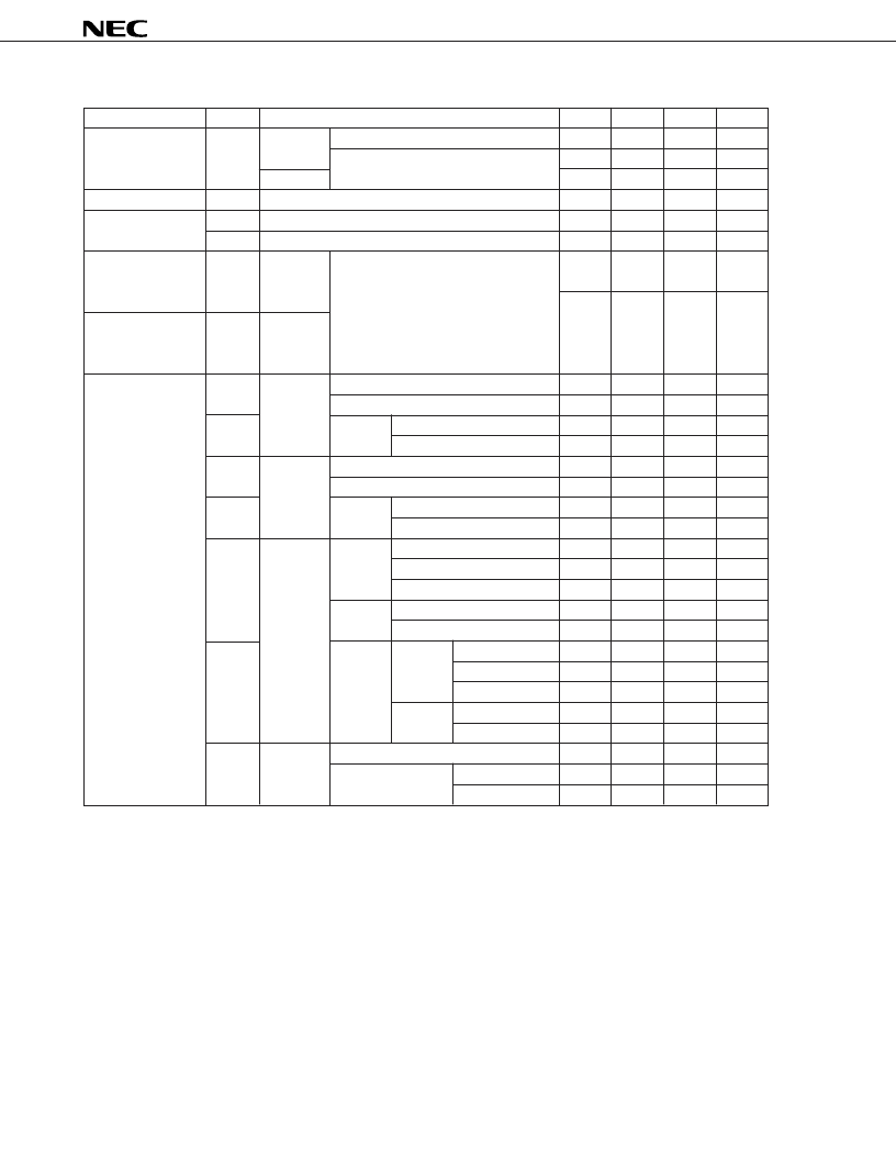
60
μ
PD753036, 753036(A)
Data Sheet U11353EJ4V0DS00
DC Characteristics (T
A
= –40 to +85
°
C, V
DD
= 1.8 to 5.5 V)
Parameter
Symbol
Conditions
MIN.
TYP.
MAX.
Unit
LCD drive voltage
V
LCD
VAC0 = 0
T
A
= –40 to +85
°
C
T
A
= –10 to 85
°
C
2.7
V
DD
V
2.2
V
DD
V
VAC0 = 1
1.8
V
DD
V
VAC current
Note 1
I
VAC
VAC0 = 1, V
DD
= 2.0 V
±
10%
1
4
μ
A
k
k
LCD divider
R
LCD1
50
100
200
resistor
Note 2
R
LCD2
5
10
20
LCD output voltage
V
ODC
I
O
=
±
1.0
μ
A
V
LCD0
= V
LCD
0
±
0.2
V
deviation
Note 3
V
LCD1
= V
LCD
×
2/3
V
LCD2
= V
LCD
×
1/3
1.8 V
≤
V
LCD
≤
V
DD
(common)
LCD output voltage
V
ODS
I
O
=
±
0.5
μ
A
0
±
0.2
V
deviation
Note 3
(segment)
Supply current
Note 4
I
DD1
V
DD
= 5.0 V
±
10%
Note 6
V
DD
= 3.0 V
±
10%
Note 7
HALT
V
DD
= 5.0 V
±
10%
V
DD
= 3.0 V
±
10%
V
DD
= 5.0 V
±
10%
Note 6
V
DD
= 3.0 V
±
10%
Note 7
V
DD
= 5.0 V
±
10%
V
DD
= 3.0 V
±
10%
Low-
V
DD
= 3.0 V
±
10%
V
DD
= 2.0 V
±
10%
mode
Note 9
V
DD
= 3.0 V, T
A
= 25
°
C
V
DD
= 3.0 V
±
10%
V
DD
= 3.0 V, T
A
= 25
°
C
HALT
Low-
2.5
7.5
mA
0.6
1.8
mA
I
DD2
0.9
2.7
mA
mode
0.5
1.0
mA
I
DD1
1.7
4.5
mA
0.33
1.0
mA
I
DD2
HALT
0.7
2.0
mA
mode
0.3
0.9
mA
I
DD3
12
35
μ
A
μ
A
μ
A
μ
A
μ
A
μ
A
μ
A
μ
A
μ
A
μ
A
μ
A
μ
A
μ
A
voltage
5.5
16
12
24
9.2
27
9.2
18
I
DD4
V
DD
= 3.0 V
±
10%
V
DD
= 2.0 V
±
10%
8.5
25
mode
voltage
3.0
12.0
mode
Note 9
Low power
consumption
mode
Note 10
V
DD
= 3.0 V, T
A
= 25
°
C
8.5
17
V
DD
= 3.0 V
±
10%
4.6
13.8
V
DD
= 3.0 V, T
A
= 25
°
C
4.6
9.2
I
DD5
XT1 =
V
DD
= 5.0 V
±
10%
V
DD
= 3.0 V
±
10%
0.05
10
0 V
Note 11
0.02
5.0
STOP mode
T
A
= 25
°
C
0.02
3.0
Notes 1.
Clear VAC0 to 0 in the low-current mode and STOP mode. When VAC0 is set to 1, the current increases
by about 1
μ
A.
Either R
LCD1
or R
LCD2
can be selected by mask option.
Voltage deviation is the difference between the ideal values (V
LCDn
; n = 0, 1, 2) of the segment and
common outputs and the output voltage.
The current flowing through the internal pull-up resistor and the LCD divider resistor is not included.
Including the case when the subsystem clock oscillates.
When the device operates in high-speed mode with the processor clock control register (PCC) set to 0011.
When the device operates in low-speed mode with PCC set to 0000.
When the device operates on the subsystem clock, with the system clock control register (SCC) set
to 1001 and oscillation of the main system clock stopped.
When the sub-oscillator control register (SOS) is set to 0000.
10.
When SOS is set to 0010.
11.
When SOS is set to 00
×
1 and the sub-oscillator feedback resistor is not used (
×
: don’t care).
2.
3.
4.
5.
6.
7.
8.
9.
32.768
kHz
Note 8
crystal
oscillation
Low current
consumption
mode
Note 10
6.00 MHz
Note 5
crystal
oscillation
C1 = C2
= 22 pF
4.19 MHz
Note 5
crystal
oscillation
C1 = C2
= 22 pF
相關PDF資料 |
PDF描述 |
|---|---|
| UPD753036GCA | DIODE ZENER SINGLE 500mW 60Vz 2.1mA-Izt 0.05 0.1uA-Ir 46Vr DO35-GLASS 5K/REEL |
| UPD753036GK | DIODE ZENER SINGLE 500mW 75Vz 1.7mA-Izt 0.05 0.1uA-Ir 56Vr DO35-GLASS 5K/REEL |
| UPD753104 | 4-BIT SINGLE-CHIP MICROCONTROLLER FOR SMALL GENERAL-PURPOSE INFRARED REMOTE CONTROL TRANSMITTER |
| UPD753104GC | 4-BIT SINGLE-CHIP MICROCONTROLLER FOR SMALL GENERAL-PURPOSE INFRARED REMOTE CONTROL TRANSMITTER |
| UPD753104GK | 4-BIT SINGLE-CHIP MICROCONTROLLER FOR SMALL GENERAL-PURPOSE INFRARED REMOTE CONTROL TRANSMITTER |
相關代理商/技術參數(shù) |
參數(shù)描述 |
|---|---|
| UPD75304GF-407-3B9 | 制造商:Renesas Electronics Corporation 功能描述: |
| UPD75306G182 | 制造商:Panasonic Industrial Company 功能描述:IC |
| UPD75308F478 | 制造商:Panasonic Industrial Company 功能描述:IC |
| UPD75308G699 | 制造商:Panasonic Industrial Company 功能描述:IC |
| UPD753204013 | 制造商:Panasonic Industrial Company 功能描述:IC |
發(fā)布緊急采購,3分鐘左右您將得到回復。