- 您現(xiàn)在的位置:買賣IC網(wǎng) > PDF目錄378747 > UPD75518 (NEC Corp.) 4 BIT SINGLE-CHIP MICROCOMPUTER PDF資料下載
參數(shù)資料
| 型號(hào): | UPD75518 |
| 廠商: | NEC Corp. |
| 英文描述: | 4 BIT SINGLE-CHIP MICROCOMPUTER |
| 中文描述: | 4位單片機(jī) |
| 文件頁數(shù): | 102/180頁 |
| 文件大?。?/td> | 1595K |
| 代理商: | UPD75518 |
第1頁第2頁第3頁第4頁第5頁第6頁第7頁第8頁第9頁第10頁第11頁第12頁第13頁第14頁第15頁第16頁第17頁第18頁第19頁第20頁第21頁第22頁第23頁第24頁第25頁第26頁第27頁第28頁第29頁第30頁第31頁第32頁第33頁第34頁第35頁第36頁第37頁第38頁第39頁第40頁第41頁第42頁第43頁第44頁第45頁第46頁第47頁第48頁第49頁第50頁第51頁第52頁第53頁第54頁第55頁第56頁第57頁第58頁第59頁第60頁第61頁第62頁第63頁第64頁第65頁第66頁第67頁第68頁第69頁第70頁第71頁第72頁第73頁第74頁第75頁第76頁第77頁第78頁第79頁第80頁第81頁第82頁第83頁第84頁第85頁第86頁第87頁第88頁第89頁第90頁第91頁第92頁第93頁第94頁第95頁第96頁第97頁第98頁第99頁第100頁第101頁當(dāng)前第102頁第103頁第104頁第105頁第106頁第107頁第108頁第109頁第110頁第111頁第112頁第113頁第114頁第115頁第116頁第117頁第118頁第119頁第120頁第121頁第122頁第123頁第124頁第125頁第126頁第127頁第128頁第129頁第130頁第131頁第132頁第133頁第134頁第135頁第136頁第137頁第138頁第139頁第140頁第141頁第142頁第143頁第144頁第145頁第146頁第147頁第148頁第149頁第150頁第151頁第152頁第153頁第154頁第155頁第156頁第157頁第158頁第159頁第160頁第161頁第162頁第163頁第164頁第165頁第166頁第167頁第168頁第169頁第170頁第171頁第172頁第173頁第174頁第175頁第176頁第177頁第178頁第179頁第180頁
102
μ
PD75518(A)
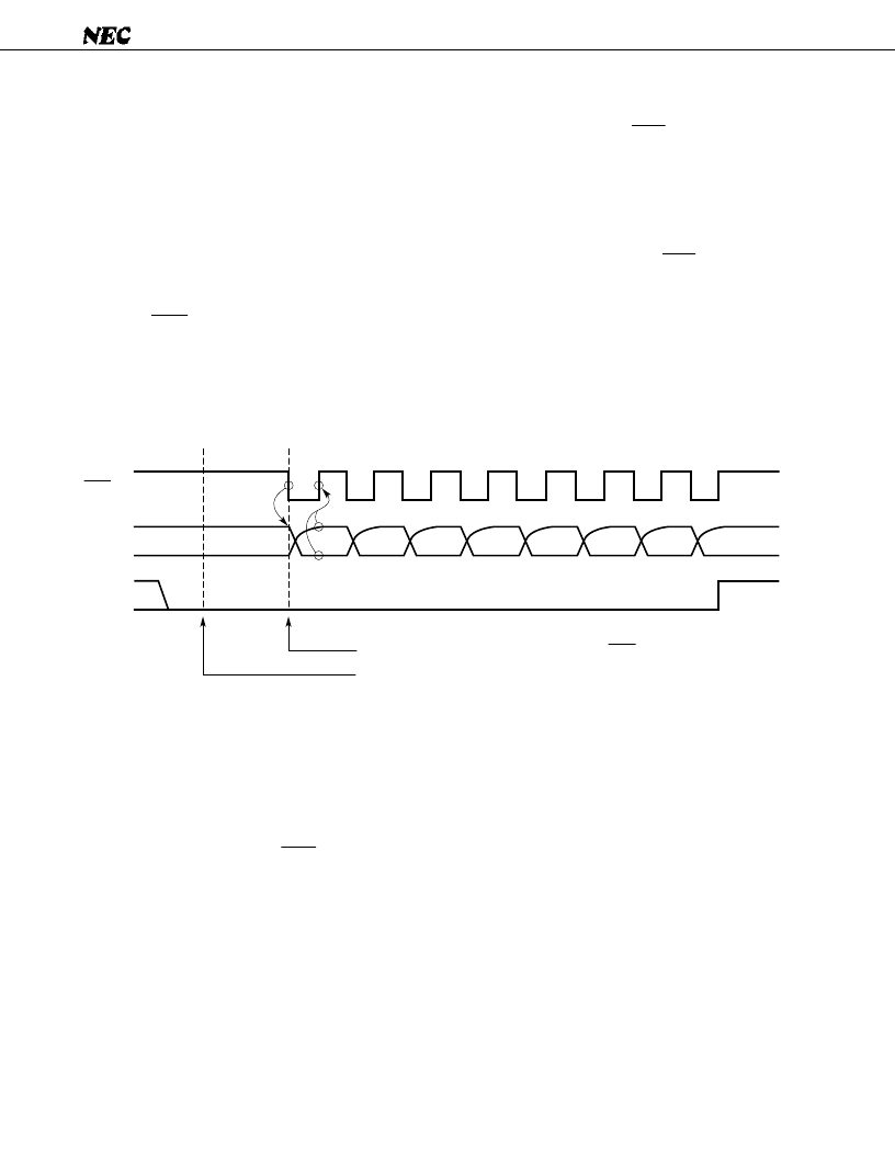
(3) Two-wire serial I/O mode
The two-wire serial I/O mode can be made compatible with any communication format by programming.
In this mode, communication is basically performed using two lines: Serial clock (SCK0) and serial data
input/output (SB0 or SB1).
(a) Communication operation
The two-wire serial I/O mode transfers data, with eight bits as one block. Data is transferred bit by
bit in phase with the serial clock.
The shift register 0 performs shift operation on the falling edge of the serial clock (SCK0). Transmit
data is latched on the SO0 latch, and is output on the SB0/P02 pin or SB1/P03 pin starting with the
MSB. Receive data applied to the SB0 pin or SB1 pin is latched in the shift register on the rising edge
of SCK0.
When eight bits have been transferred, shift register 0 operation automatically terminates setting the
interrupt request flag (IRQCSI0).
Fig. 4-46 Timing of Two-Wire Serial I/O Mode
The SB0 or SB1 pin becomes an N-ch open-drain I/O when specified as the serial data bus, so the
voltage level on that pin must be pulled up externally.
The state of the SO0 latch is output on the SB0 or SB1 pin, so the SB0 or SB1 pin output states can
be controlled by setting the RELT or CMDT bit.
However, this operation must not be performed during serial transfer.
The output state of the SCK0 pin can be controlled by manipulating the P01 output latch in the output
mode (internal system clock mode). (See
Section 4.8.7
.)
SCK0
SB0/SB1
IRQCSI0
1
2
3
4
5
6
7
8
D0
D1
D2
D3
D4
D5
D6
D7
Transfer is started in phase with falling edge of SCK0.
Execution of instruction that writes date to SIO0 (Transfer start request)
Completion of transfer
相關(guān)PDF資料 |
PDF描述 |
|---|---|
| UPD75518GF | CAT5E PATCH CABLES SNAGLESS, RED 3 FT |
| UPD75518GFA | 4 BIT SINGLE-CHIP MICROCOMPUTER |
| UPD75518A | 4 BIT SINGLE-CHIP MICROCOMPUTER |
| UPD7556 | 4-BIT, SINGLE-CHIP CMOS MICROCOMPUTERS WITH COMPARATOR |
| UPD7566CS | 4-BIT, SINGLE-CHIP CMOS MICROCOMPUTERS WITH COMPARATOR |
相關(guān)代理商/技術(shù)參數(shù) |
參數(shù)描述 |
|---|---|
| UPD7554AG-597-E2 | 制造商:Renesas Electronics Corporation 功能描述: |
| UPD7554AG-597-E2-A | 制造商:Renesas Electronics Corporation 功能描述: |
| UPD7554AG-603-E2 | 制造商:Renesas Electronics Corporation 功能描述: |
| UPD7554AG-603-E2-A | 制造商:Renesas Electronics Corporation 功能描述: |
| UPD7554AG-611-E2 | 制造商:Renesas Electronics Corporation 功能描述: |
發(fā)布緊急采購,3分鐘左右您將得到回復(fù)。