- 您現(xiàn)在的位置:買賣IC網(wǎng) > PDF目錄378747 > UPD75518 (NEC Corp.) 4 BIT SINGLE-CHIP MICROCOMPUTER PDF資料下載
參數(shù)資料
| 型號: | UPD75518 |
| 廠商: | NEC Corp. |
| 英文描述: | 4 BIT SINGLE-CHIP MICROCOMPUTER |
| 中文描述: | 4位單片機 |
| 文件頁數(shù): | 87/180頁 |
| 文件大小: | 1595K |
| 代理商: | UPD75518 |
第1頁第2頁第3頁第4頁第5頁第6頁第7頁第8頁第9頁第10頁第11頁第12頁第13頁第14頁第15頁第16頁第17頁第18頁第19頁第20頁第21頁第22頁第23頁第24頁第25頁第26頁第27頁第28頁第29頁第30頁第31頁第32頁第33頁第34頁第35頁第36頁第37頁第38頁第39頁第40頁第41頁第42頁第43頁第44頁第45頁第46頁第47頁第48頁第49頁第50頁第51頁第52頁第53頁第54頁第55頁第56頁第57頁第58頁第59頁第60頁第61頁第62頁第63頁第64頁第65頁第66頁第67頁第68頁第69頁第70頁第71頁第72頁第73頁第74頁第75頁第76頁第77頁第78頁第79頁第80頁第81頁第82頁第83頁第84頁第85頁第86頁當前第87頁第88頁第89頁第90頁第91頁第92頁第93頁第94頁第95頁第96頁第97頁第98頁第99頁第100頁第101頁第102頁第103頁第104頁第105頁第106頁第107頁第108頁第109頁第110頁第111頁第112頁第113頁第114頁第115頁第116頁第117頁第118頁第119頁第120頁第121頁第122頁第123頁第124頁第125頁第126頁第127頁第128頁第129頁第130頁第131頁第132頁第133頁第134頁第135頁第136頁第137頁第138頁第139頁第140頁第141頁第142頁第143頁第144頁第145頁第146頁第147頁第148頁第149頁第150頁第151頁第152頁第153頁第154頁第155頁第156頁第157頁第158頁第159頁第160頁第161頁第162頁第163頁第164頁第165頁第166頁第167頁第168頁第169頁第170頁第171頁第172頁第173頁第174頁第175頁第176頁第177頁第178頁第179頁第180頁
87
μ
PD75518(A)
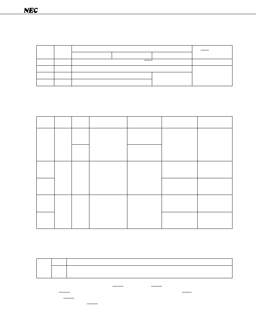
Fig. 4-35 Format of Serial Operation Mode Register 0 (CSIM0) (2/3)
Serial clock selection bit (W)
Note
The values in parentheses are for f
X
= 4.19 MHz or 6.0 MHz.
Serial interface operation mode selection bit (W)
Remark
×
: Don’t care
Wake-up function specification bit (W)
Caution When WUP = 1 is set during BUSY signal output, BUSY is not released. In the SBI mode, the
BUSY signal is output until the next falling edge of the serial clock (SCK0) appears after release
of BUSY is directed. Before setting WUP = 1, be sure to confirm that the SB0 (or SB1) pin is high
after releasing BUSY.
Serial clock
SBI mode
2-wire serial I/O mode
3-wire serial I/O mode
External clock applied to SCK0 pin
Timer/event counter output (T0)
f
X
/2
4
(262 kHz or 375 kHz)
Note
f
X
/2
3
(524 kHz or 750 kHz)
Note
CSIM01
CSIM00
f
X
/2
6
(65.5 kHz or
93.8 kHz)
Note
SCK0 pin mode
0
0
1
1
0
1
0
1
Input
Output
Operation mode
CSIM04
CSIM03
CSIM02
Shift register bit
sequence
SIO0
7-0
XA
(Transfer starting
with MSB)
SIO0
0-7
XA
(Transfer starting
with LSB)
SIO0
7-0
XA
(Transfer starting
with MSB)
SIO0
7-0
XA
(Transfer starting
with MSB)
SI0 pin function
0
1
1
0
1
0
1
×
0
1
0
1
SO0 pin function
SO0/P02
(CMOS output)
SB0/P02
(N-ch open-drain
input/output)
P02 input
SB0/P02
(N-ch open-drain
input/output)
P02 input
SI0/P03
(Input)
P03 input
SB1/P03
(N-ch open-drain
input/output)
P03 input
SB1/P03
(N-ch open-drain
input/output)
3-wire serial I/O
mode
SBI mode
2-wire serial I/O
mode
Sets IRQCSI0 each time serial transfer is completed in each mode.
Used in the SBI mode only to set IRQCSI0 only when an address received after bus release matches
the data in the slave address register (wake-up state). SB0/SB1 goes to high-impedance state.
WUP
0
1
相關(guān)PDF資料 |
PDF描述 |
|---|---|
| UPD75518GF | CAT5E PATCH CABLES SNAGLESS, RED 3 FT |
| UPD75518GFA | 4 BIT SINGLE-CHIP MICROCOMPUTER |
| UPD75518A | 4 BIT SINGLE-CHIP MICROCOMPUTER |
| UPD7556 | 4-BIT, SINGLE-CHIP CMOS MICROCOMPUTERS WITH COMPARATOR |
| UPD7566CS | 4-BIT, SINGLE-CHIP CMOS MICROCOMPUTERS WITH COMPARATOR |
相關(guān)代理商/技術(shù)參數(shù) |
參數(shù)描述 |
|---|---|
| UPD7554AG-597-E2 | 制造商:Renesas Electronics Corporation 功能描述: |
| UPD7554AG-597-E2-A | 制造商:Renesas Electronics Corporation 功能描述: |
| UPD7554AG-603-E2 | 制造商:Renesas Electronics Corporation 功能描述: |
| UPD7554AG-603-E2-A | 制造商:Renesas Electronics Corporation 功能描述: |
| UPD7554AG-611-E2 | 制造商:Renesas Electronics Corporation 功能描述: |
發(fā)布緊急采購,3分鐘左右您將得到回復。