- 您現(xiàn)在的位置:買賣IC網(wǎng) > PDF目錄225499 > V58C2128404SBLT6I (PROMOS TECHNOLOGIES INC) 32M X 4 DDR DRAM, 0.7 ns, PDSO66 PDF資料下載
參數(shù)資料
| 型號(hào): | V58C2128404SBLT6I |
| 廠商: | PROMOS TECHNOLOGIES INC |
| 元件分類: | DRAM |
| 英文描述: | 32M X 4 DDR DRAM, 0.7 ns, PDSO66 |
| 封裝: | 0.400 X 0.875 INCH, PLASTIC, MS-024FC, TSOP2-66 |
| 文件頁數(shù): | 30/60頁 |
| 文件大小: | 915K |
| 代理商: | V58C2128404SBLT6I |
第1頁第2頁第3頁第4頁第5頁第6頁第7頁第8頁第9頁第10頁第11頁第12頁第13頁第14頁第15頁第16頁第17頁第18頁第19頁第20頁第21頁第22頁第23頁第24頁第25頁第26頁第27頁第28頁第29頁當(dāng)前第30頁第31頁第32頁第33頁第34頁第35頁第36頁第37頁第38頁第39頁第40頁第41頁第42頁第43頁第44頁第45頁第46頁第47頁第48頁第49頁第50頁第51頁第52頁第53頁第54頁第55頁第56頁第57頁第58頁第59頁第60頁
36
V58C2128(804/404/164)SB*I Rev. 1.3 March 2006
ProMOS TECHNOLOGIES
V58C2128(804/404/164)SB*I
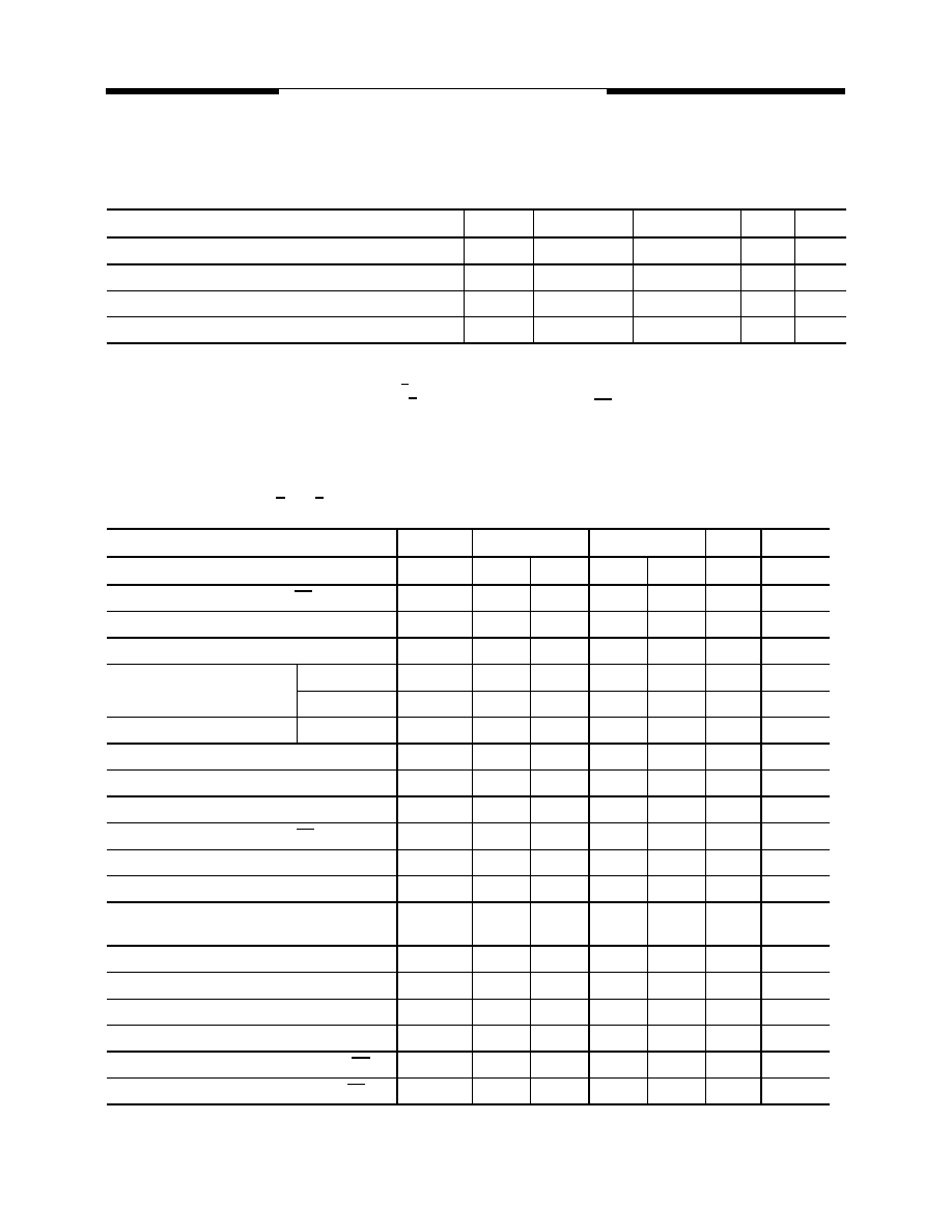
AC Operating Conditions & Timing Specification
AC Operating Conditions
Note:
1.Vih(max) = 4.2V. The overshoot voltage duration is < 3ns at VDD.
2. Vil(min) = -1.5V. The undershoot voltage duration is < 3ns at VSS.
3. VID is the magnitude of the difference between the input level on CK and the input on CK.
4. The value of VIX is expected to equal 0.5*VDDQ of the transmitting device and must track variations in the DC level of the same.
ELECTRICAL CHARACTERISTICS AND AC TIMING for PC400/PC333 -Absolute Specifica-
tions
(Notes: 1-5, 14-17) (-40°C < T A < +85°C; VDDQ = +2.5V ±0.2V, VDD=+2.5V ±0.2V for DDR400 device VDDQ = +2.6V
±0.1V, VDD=+2.6V ±0.1V)
Parameter/Condition
Symbol
Min
Max
Unit
Note
Input High (Logic 1) Voltage, DQ, DQS and DM signals
VIH(AC)
VREF + 0.31
V
1
Input Low (Logic 0) Voltage, DQ, DQS and DM signals.
VIL(AC)
VREF - 0.31
V
2
Input Differential Voltage, CK and CK inputs
VID(AC)
0.7
VDDQ+0.6
V
3
Input Crossing Point Voltage, CK and CK inputs
VIX(AC)
0.5*VDDQ-0.2
0.5*VDDQ+0.2
V
4
AC CHARACTERISTICS
-5
-6
PARAMETER
SYMBOL
MIN
MAX
MIN
MAX
UNITS
NOTES
Access window of DQs from CK/CK
tAC
-0.65
0.65
-0.7
0.7
ns
CK high-level width
tCH
0.45
0.55
0.45
0.55
tCK
30
CK low-level width
tCL
0.45
0.55
0.45
0.55
tCK
30
Clock cycle time
CL = 3
tCK (3)
5
10
-
12
ns
52
CL = 2.5
tCK (2.5)
6
10
6
12
ns
52
CL = 2
tCK (2)
7.5
10
7.5
12
ns
52
DQ and DM input hold time relative to DQS
tDH
0.40
0.45
ns
26,31
DQ and DM input setup time relative to DQS
tDS
0.40
0.45
ns
26,31
DQ and DM input pulse width (for each input)
tDIPW
1.75
ns
31
Access window of DQS from CK/CK
tDQSCK
-0.6
0.6
-0.6
0.6
ns
DQS input high pulse width
tDQSH
0.35
tCK
DQS input low pulse width
tDQSL
0.35
tCK
DQS-DQ skew, DQS to last DQ valid,
per group, per access
tDQSQ
0.40
0.45
ns
25,26
Write command to first DQS latching transition
tDQSS
0.72
1.25
0.75
1.25
tCK
DQS falling edge to CK rising - setup time
tDSS
0.2
tCK
DQS falling edge from CK rising - hold time
tDSH
0.2
tCK
Half clock period
tHP
tCH, tCL
ns
34
Data-out high-impedance window from CK/CK
tHZ
-0.65
+0.65
-0.7
+0.7
ns
18
Data-out low-impedance window from CK/CK
tLZ
-0.65
+0.65
-0.7
+0.7
ns
18
相關(guān)PDF資料 |
PDF描述 |
|---|---|
| V58C365164S5 | 4M X 16 DDR DRAM, 0.1 ns, PDSO66 |
| V608ME06 | VCO, 1900 MHz - 2270 MHz |
| V603ME07 | VCO, 1896 MHz - 1924 MHz |
| V6049001 | VCO, 1600 MHz - 2200 MHz |
| V610ME04 | VCO, 1950 MHz - 2150 MHz |
相關(guān)代理商/技術(shù)參數(shù) |
參數(shù)描述 |
|---|---|
| V58C2128804S | 制造商:MOSEL 制造商全稱:MOSEL 功能描述:HIGH PERFORMANCE 2.5 VOLT 128 Mbit DDR SDRAM |
| V58C2256 | 制造商:MOSEL 制造商全稱:MOSEL 功能描述:HIGH PERFORMANCE 2.5 VOLT 256 Mbit DDR SDRAM |
| V58C2256164S | 制造商:MOSEL 制造商全稱:MOSEL 功能描述:HIGH PERFORMANCE 2.5 VOLT 256 Mbit DDR SDRAM |
| V58C2256324SAB30 | 制造商:Marvell 功能描述:Marvell V58C2256324SAB30 |
| V58C2256324SAB33 | 制造商:Marvell 功能描述:Marvell V58C2256324SAB33 |
發(fā)布緊急采購,3分鐘左右您將得到回復(fù)。