- 您現(xiàn)在的位置:買賣IC網(wǎng) > PDF目錄376455 > XR17L152IM (EXAR CORP) CAP .068UF 400V PEN FILM 2825 5% PDF資料下載
參數(shù)資料
| 型號: | XR17L152IM |
| 廠商: | EXAR CORP |
| 元件分類: | 微控制器/微處理器 |
| 英文描述: | CAP .068UF 400V PEN FILM 2825 5% |
| 中文描述: | 2 CHANNEL(S), 3.125M bps, SERIAL COMM CONTROLLER, PQFP100 |
| 封裝: | 14 X 14 MM, 1 MM HEIGHT, TQFP-100 |
| 文件頁數(shù): | 15/55頁 |
| 文件大?。?/td> | 318K |
| 代理商: | XR17L152IM |
第1頁第2頁第3頁第4頁第5頁第6頁第7頁第8頁第9頁第10頁第11頁第12頁第13頁第14頁當(dāng)前第15頁第16頁第17頁第18頁第19頁第20頁第21頁第22頁第23頁第24頁第25頁第26頁第27頁第28頁第29頁第30頁第31頁第32頁第33頁第34頁第35頁第36頁第37頁第38頁第39頁第40頁第41頁第42頁第43頁第44頁第45頁第46頁第47頁第48頁第49頁第50頁第51頁第52頁第53頁第54頁第55頁

XR17L152
3.3V PCI BUS DUAL UART
REV. 1.1.0
á
DISCONTINUED
15
1.2.6
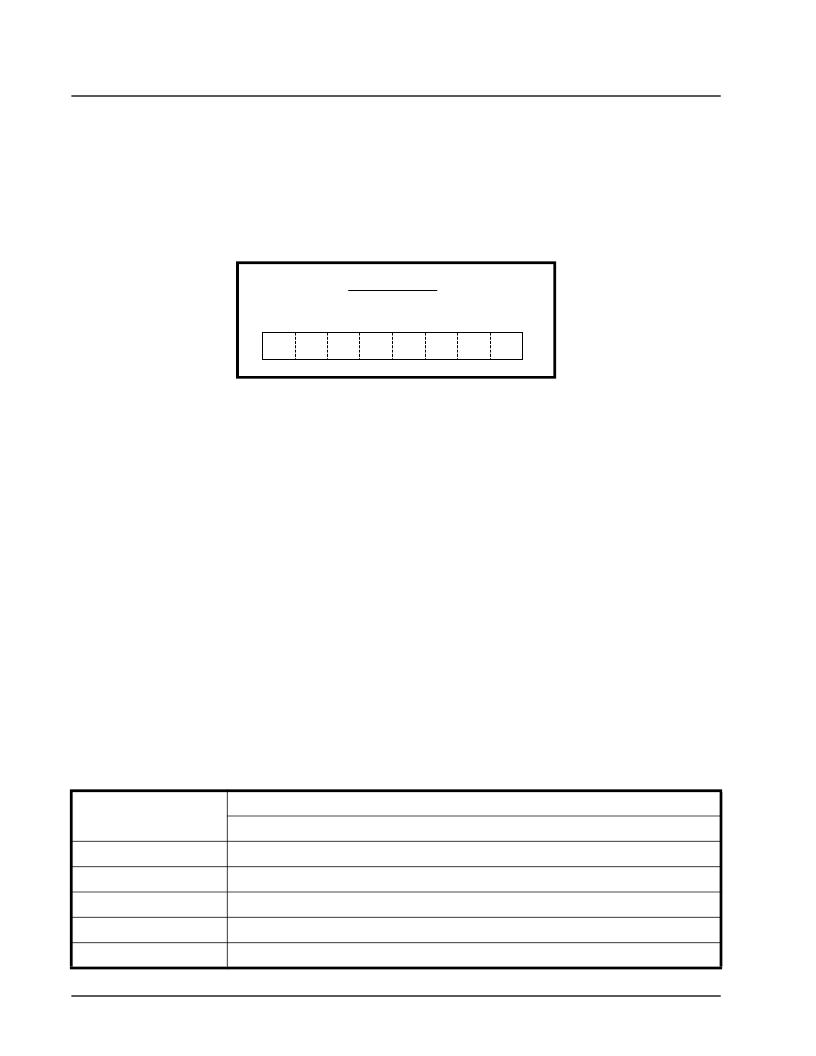
The first two bits of the Sleep register enables each UART channel separately to enter Sleep mode. The upper
bits 2 to 7 are reserved. Sleep mode reduces power consumption when the system needs to put the UART(s)
to idle. The UART enters Sleep mode when there is no interrupt pending. When both UARTs are put to sleep,
the on-chip oscillator shuts off to further conserve power. In this case, the XR17L152 is awakened on any of
the channels by a receive data byte or a change on the serial port. The UART is ready after 32 crystal clocks
to
ensure full functionality. Also, a special interrupt is generated with an indication of no pending interrupt. Logic 0
(default) disables sleep mode and logic 1 enables it.
SLEEP [31:24] - (default 0x00)
1.2.7
There are 2 internal registers that provide device identification and revision, DVID and DREV registers. The 8-
bit content in the DVID register provides device identification. A return value of 0x22 from this register indicates
the device is an XR17C152 or an XR17L152. The DREV register returns an 8-bit value of 0x01 for revision A
with 0x02 equals to revision B and so forth. This information is very useful to the software driver for identifying
which device it is communicating with and to keep up with revision changes.
DVID [15:8]
Device identification for the type of UART. The upper nibble indicates it is an XR17Cxxx or XR17Lxxx series
device with lower nibble indicating the number of channels.
Examples:
XR17C158 = 0x28
XR17C154 or XR17L154 = 0x24
XR17C152 or XR17L152 = 0x22
DREV [7:0]
Revision number of the XR17L152. A 0x01 represents "revision-A" with 0x02 for rev-B and so forth.
REGB [23:16] (default 0x00)
REGB register provides a control for simultaneous write to both UARTs configuration register or individually.
This is very useful for device initialization in the power up and reset routines. Also, the register provides a
facility to interface to the non-volatile memory device such as a 93C46 EEPROM. In embedded applications,
the user can use this facility to store proprietary data.
Device Identification and Revision
1.2.8
REGB Register
REGB[16] (Read/Write)
Logic 0 (default) write to each UART configuration registers individually.
Logic 1 enables simultaneous write to both UARTs configuration register.
REGB[19:17]
Reserved.
REGB[20] (Write-Only)
Control the EECK, clock, output (pin 116) on the EEPROM interface.
REGB[21] (Write-Only)
Control the EECS, chips select, output (pin 115) to the EEPROM device.
REGB[22] (Write-Only)
EEDI (pin 114) data input. Write data to the EEPROM device.
REGB[23] (Read-Only)
EEDO (pin 113) data output. Read data from the EEPROM device.
SLEEP Register
Individual UART Channel Sleep Enable
Bit-7 Bit-6 Bit-5 Bit-4 Bit-3 Bit-2 Bit-1 Bit-0
Rsvd
Rsvd Rsvd Ch-1 Ch-0
Rsvd Rsvd Rsvd
相關(guān)PDF資料 |
PDF描述 |
|---|---|
| XR17L152 | 3.3V PCI BUS DUAL UART |
| XR17L152CM | 3.3V PCI BUS DUAL UART |
| XR2001 | High-Voltage, High-Current Darlington Transistor Arrays |
| XR2002CN | High-Voltage, High-Current Darlington Transistor Arrays |
| XR2003 | High-Voltage, High-Current Darlington Transistor Arrays |
相關(guān)代理商/技術(shù)參數(shù) |
參數(shù)描述 |
|---|---|
| XR17L154 | 制造商:EXAR 制造商全稱:EXAR 功能描述:3.3V PCI BUS QUAD UART |
| XR17L154CV | 制造商:未知廠家 制造商全稱:未知廠家 功能描述:Telecomm/Datacomm |
| XR17L154IV | 制造商:EXAR 制造商全稱:EXAR 功能描述:3.3V PCI BUS QUAD UART |
| XR17V252 | 制造商:EXAR 制造商全稱:EXAR 功能描述:66 MHZ PCI BUS DUAL UART WITH POWER MANAGEMENT SUPPORT |
| XR17V252_08 | 制造商:EXAR 制造商全稱:EXAR 功能描述:66 MHZ PCI BUS DUAL UART WITH POWER MANAGEMENT SUPPORT |
發(fā)布緊急采購,3分鐘左右您將得到回復(fù)。