- 您現(xiàn)在的位置:買賣IC網(wǎng) > PDF目錄376462 > XRT75L00DIV (EXAR CORP) E3/DS3/STS-1 LINE INTERFACE UNIT WITH SONET DESYNCHRONIZER PDF資料下載
參數(shù)資料
| 型號: | XRT75L00DIV |
| 廠商: | EXAR CORP |
| 元件分類: | 數(shù)字傳輸電路 |
| 英文描述: | E3/DS3/STS-1 LINE INTERFACE UNIT WITH SONET DESYNCHRONIZER |
| 中文描述: | DATACOM, PCM TRANSCEIVER, PQFP52 |
| 封裝: | 10 X 10 MM, TQFP-52 |
| 文件頁數(shù): | 85/92頁 |
| 文件大小: | 894K |
| 代理商: | XRT75L00DIV |
第1頁第2頁第3頁第4頁第5頁第6頁第7頁第8頁第9頁第10頁第11頁第12頁第13頁第14頁第15頁第16頁第17頁第18頁第19頁第20頁第21頁第22頁第23頁第24頁第25頁第26頁第27頁第28頁第29頁第30頁第31頁第32頁第33頁第34頁第35頁第36頁第37頁第38頁第39頁第40頁第41頁第42頁第43頁第44頁第45頁第46頁第47頁第48頁第49頁第50頁第51頁第52頁第53頁第54頁第55頁第56頁第57頁第58頁第59頁第60頁第61頁第62頁第63頁第64頁第65頁第66頁第67頁第68頁第69頁第70頁第71頁第72頁第73頁第74頁第75頁第76頁第77頁第78頁第79頁第80頁第81頁第82頁第83頁第84頁當前第85頁第86頁第87頁第88頁第89頁第90頁第91頁第92頁

XRT75L00D
REV. 1.0.2
E3/DS3/STS-1 LINE INTERFACE UNIT WITH SONET DESYNCHRONIZER
80
induced "stuffed-byte", the POH byte, and the two fixed-stuff bytes within the STS-1 SPE, etc), immediately
followed be processing clusters of DS3 data-bits (as shown in Figure 37) and still comply with the "Category I
Intrinsic Jitter Requirements per Telcordia GR-253-CORE for DS3 applications.
N
OTE
:
If this sort of "pre-processing" is already supported by the Mapper device that you are using, then no further action
is required by the user.
9.8.2.2
OUR PRE-PROCESSING RECOMMENDATIONS
For the time-being, we recommend that the customer implement the "pre-processing" of the DS3 "Data-Signal"
and "Clock-Signal" as described below. Currently we are aware that some of the Mapper products on the
Market do implement this exact "pre-processing" algorithm. However, if the customer is implementing their
Mapper Design in an ASIC or FPGA solution, then we strongly recommend that the user implement the
necessary logic design to realize the following recommendations.
Some time ago, we spent some time, studying (and then later testing our solution with) the PM5342 OC-3 to
DS3 Mapper IC from PMC-Sierra. In particular, we wanted to understand the type of "DS3 Clock" and "Data"
signal that this DS3 to OC-3 Mapper IC outputs.
During this effort, we learned the following.
1.
This "DS3 Clock" and "Data" signal, which is output from the Mapper IC consists of two major "repeating"
patterns (which we will refer to as "MAJOR PATTERN A" and "MAJOR PATTERN B". The behavior of
each of these patterns is presented below.
MAJOR PATTERN A
MAJOR PATTERN A consists of two "sub" or minor-patterns, (which we will refer to as "MINOR PATTERN P1
and P2).
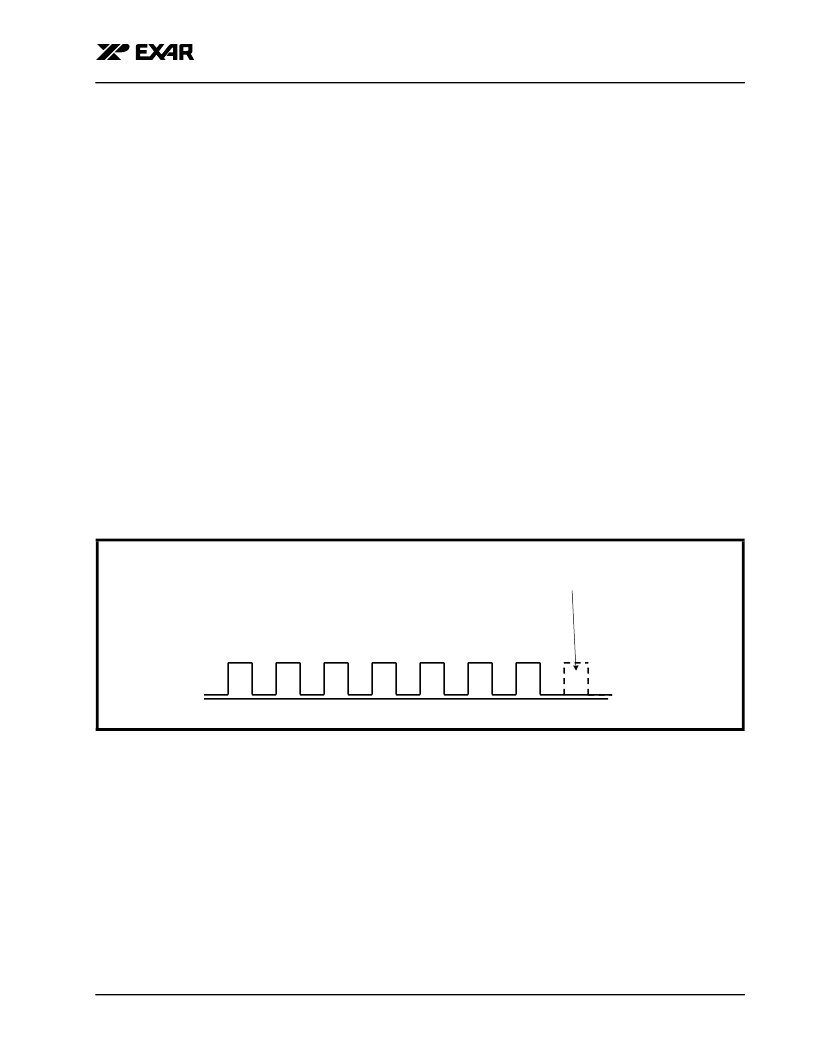
MINOR PATTERN P1 consists of a string of seven (7) clock pulses, followed by a single gap (no clock pulse).
An illustration of MINOR PATTERN P1 is presented below in Figure 58.
It should be noted that each of these clock pulses has a period of approximately 19.3ns (or has an
"instantaneously frequency of 51.84MHz).
MINOR Pattern P2 consists of string of five (5) clock pulses, which is also followed by a single gap (no clock
pulse). An illustration of Pattern P2 is presented below in Figure 59.
F
IGURE
58. I
LLUSTRATION
OF
MINOR PATTERN P1
1 2 3 4 5
6 7
Missing Clock Pulse
相關(guān)PDF資料 |
PDF描述 |
|---|---|
| XRT75L02 | TWO CHANNEL E3/DS3/STS-1 LINE INTERFACE UNIT WITH JITTER |
| XRT75L02IV | TWO CHANNEL E3/DS3/STS-1 LINE INTERFACE UNIT WITH JITTER |
| XRT75L03D | THREE CHANNEL E3/DS3/STS-1 LINE INTERFACE UNIT WITH SONET DESYNCHRONIZER |
| XRT75L04D | FOUR CHANNEL E3/DS3/STS-1 LINE INTERFACE UNIT WITH SONET DESYNCHRONIZER |
| XRT75L04DIV | FOUR CHANNEL E3/DS3/STS-1 LINE INTERFACE UNIT WITH SONET DESYNCHRONIZER |
相關(guān)代理商/技術(shù)參數(shù) |
參數(shù)描述 |
|---|---|
| XRT75L00DIV-F | 功能描述:外圍驅(qū)動器與原件 - PCI 1-Ch DS3, E3, SONET RoHS:否 制造商:PLX Technology 工作電源電壓: 最大工作溫度: 安裝風(fēng)格:SMD/SMT 封裝 / 箱體:FCBGA-1156 封裝:Tray |
| XRT75L00DIVTR | 功能描述:時鐘合成器/抖動清除器 3.3V 1 CH E3/DS3/STS W/SONET DE-SYNCH RoHS:否 制造商:Skyworks Solutions, Inc. 輸出端數(shù)量: 輸出電平: 最大輸出頻率: 輸入電平: 最大輸入頻率:6.1 GHz 電源電壓-最大:3.3 V 電源電壓-最小:2.7 V 封裝 / 箱體:TSSOP-28 封裝:Reel |
| XRT75L00DIVTR-F | 功能描述:時鐘合成器/抖動清除器 3.3V 1 CH E3/DS3/STS W/SONET DE-SYNCH RoHS:否 制造商:Skyworks Solutions, Inc. 輸出端數(shù)量: 輸出電平: 最大輸出頻率: 輸入電平: 最大輸入頻率:6.1 GHz 電源電壓-最大:3.3 V 電源電壓-最小:2.7 V 封裝 / 箱體:TSSOP-28 封裝:Reel |
| XRT75L00ES | 功能描述:時鐘合成器/抖動清除器 1CH T3/E3/STS1 LIU+JA 3.3V RoHS:否 制造商:Skyworks Solutions, Inc. 輸出端數(shù)量: 輸出電平: 最大輸出頻率: 輸入電平: 最大輸入頻率:6.1 GHz 電源電壓-最大:3.3 V 電源電壓-最小:2.7 V 封裝 / 箱體:TSSOP-28 封裝:Reel |
| XRT75L00IV | 功能描述:外圍驅(qū)動器與原件 - PCI 3.3V 1 CH E3/DS3/STS W/JITTER ATTEN RoHS:否 制造商:PLX Technology 工作電源電壓: 最大工作溫度: 安裝風(fēng)格:SMD/SMT 封裝 / 箱體:FCBGA-1156 封裝:Tray |
發(fā)布緊急采購,3分鐘左右您將得到回復(fù)。