- 您現(xiàn)在的位置:買賣IC網(wǎng) > PDF目錄372956 > XWM8191CFT (Wolfson Microelectronics) 14-bit 6MSPS CIS/CCD Analogue Front End/Digitiser PDF資料下載
參數(shù)資料
| 型號: | XWM8191CFT |
| 廠商: | Wolfson Microelectronics |
| 英文描述: | 14-bit 6MSPS CIS/CCD Analogue Front End/Digitiser |
| 中文描述: | 14位6MSPS獨聯(lián)體/防治荒漠化公約模擬前端/數(shù)字轉(zhuǎn)換器 |
| 文件頁數(shù): | 19/27頁 |
| 文件大小: | 355K |
| 代理商: | XWM8191CFT |
第1頁第2頁第3頁第4頁第5頁第6頁第7頁第8頁第9頁第10頁第11頁第12頁第13頁第14頁第15頁第16頁第17頁第18頁當前第19頁第20頁第21頁第22頁第23頁第24頁第25頁第26頁第27頁
Advanced Information
WM8191
WOLFSON MICROELECTRONICS LTD
AI Rev 3.1 April 2001
19
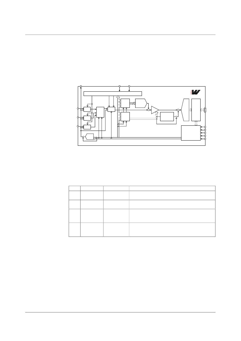
LINE-BY-LINE OPERATION
Certain linear sensors (e.g. Contact Image Sensors) give colour output on a line-by-line basis. i.e. a
full line of red pixels followed by a line of green pixels followed by a line of blue pixels. In order to
accommodate this type of signal the WM8191 can be set into Monochrome mode, with the input
channel switched by writing to control bits CHAN[1:0] between every line. Alternatively, the WM8191
can be placed into colour line-by-line mode by setting the LINEBYLINE control bit. When this bit is
set the green and blue processing channels are powered down and the device is forced internally to
only operate in MONO mode (because only one colour is sampled at a time) through the red channel.
Figure 19 shows the signal path when operating in colour line-by-line mode.
RINP
SEN/STB
SCK/RNW
VSMP
MCLK
VRLC/VBIAS
SDI/DNA
RLC/ACYC
NRESET
RLC
BINP
GINP
INPUT
MUX
OFFSET
MUX
RLC
R
G
B
R
G
B
PGA
I/P SIGNAL
POLARITY
ADJUST
8
RLC
DAC
+
CONFIGURABLE
SERIAL/
PARALLEL
CONTROL
INTERFACE
OP[13:0]
+
WM8191
14-
BIT
ADC
DATA
I/O
PORT
8
OFFSET
DAC
PGA
MUX
TIMING CONTROL
CL
V
S
R
S
4
CDS
RLC
Figure 19 Signal Path When in Line-by-Line Mode
In this mode the input multiplexer and (optionally) the PGA/Offset register multiplexers can be auto-
cycled by the application of pulses to the RLC/ACYC input pin by setting the ACYCNRLC register bit.
The multiplexers change on the first MCLK rising edge after RLC/ACYC is taken high. Alternatively,
all three multiplexers can be controlled via the serial interface by writing to register bits INTM[1:0]
to select the desired colour. It is also possible for the input multiplexer to be controlled separately
from the PGA and Offset multiplexers. Table 4 describes all the multiplexer selection modes that
are possible.
FME
0
ACYCNRLC
0
NAME
DESCRIPTION
Internal,
no force mux
Auto-cycling,
no force mux
Internal,
force mux
Input mux, offset and gain registers determined by
internal register bits INTM1, INTM0.
Input mux, offset and gain registers auto-cycled, RINP
→
GINP
→
BINP
→
RINP
…
on RLC/ACYC pulse.
Input mux selected from internal register bits FM1, FM0;
Offset and gain registers selected from internal register
bits INTM1, INTM0.
Input mux selected from internal register bits FM1, FM0;
Offset and gain registers auto-cycled, RINP
→
GINP
→
BINP
→
RINP
…
on RLC/ACYC pulse.
0
1
1
0
1
1
Auto-cycling,
force mux
Table 4 Colour Selection Description in Line-by-Line Mode
相關PDF資料 |
PDF描述 |
|---|---|
| XWM8706EDS | 24-bit, 192kHz Stereo DAC with Volume Control |
| XWM8711EDS | Internet Audio DAC with Integrated Headphone Driver |
| XWM8721EDS | Internet Audio DAC with Integrated Headphone Driver |
| XWM8722EDS | Stereo DAC with Integrated Tone Generator and Line/Variable Level Outputs |
| XWM8728EDS | 24-bit, 192kHz Stereo DAC with Volume Control and DSD Support |
相關代理商/技術參數(shù) |
參數(shù)描述 |
|---|---|
| XWM8192 | 制造商:WOLFSON 制造商全稱:WOLFSON 功能描述:(88) Bit Output 16-bit CIS/CCD AFE/Digitiser |
| XWM8192CDW/V | 制造商:WOLFSON 制造商全稱:WOLFSON 功能描述:(88) Bit Output 16-bit CIS/CCD AFE/Digitiser |
| XWM81955CFT/RV | 制造商:WOLFSON 制造商全稱:WOLFSON 功能描述:14-bit 12MSPS CIS/CCD Analogue Front End/Digitiser |
| XWM8195CFT | 制造商:WOLFSON 制造商全稱:WOLFSON 功能描述:14-bit 12MSPS CIS/CCD Analogue Front End/Digitiser |
| XWM8195SCFT/V | 功能描述:電信線路管理 IC 14Bit 12MSPS 3Ch AFE RoHS:否 制造商:STMicroelectronics 產(chǎn)品:PHY 接口類型:UART 電源電壓-最大:18 V 電源電壓-最小:8 V 電源電流:30 mA 最大工作溫度:+ 85 C 最小工作溫度:- 40 C 安裝風格:SMD/SMT 封裝 / 箱體:VFQFPN-48 封裝:Tray |
發(fā)布緊急采購,3分鐘左右您將得到回復。