- 您現在的位置:買賣IC網 > PDF目錄373785 > ZL50018 (Zarlink Semiconductor Inc.) 2 K Digital Switch with Enhanced Stratum 3 DPLL PDF資料下載
參數資料
| 型號: | ZL50018 |
| 廠商: | Zarlink Semiconductor Inc. |
| 英文描述: | 2 K Digital Switch with Enhanced Stratum 3 DPLL |
| 中文描述: | 2度數字交換機增強地層3數字鎖相環(huán) |
| 文件頁數: | 15/136頁 |
| 文件大小: | 1448K |
| 代理商: | ZL50018 |
第1頁第2頁第3頁第4頁第5頁第6頁第7頁第8頁第9頁第10頁第11頁第12頁第13頁第14頁當前第15頁第16頁第17頁第18頁第19頁第20頁第21頁第22頁第23頁第24頁第25頁第26頁第27頁第28頁第29頁第30頁第31頁第32頁第33頁第34頁第35頁第36頁第37頁第38頁第39頁第40頁第41頁第42頁第43頁第44頁第45頁第46頁第47頁第48頁第49頁第50頁第51頁第52頁第53頁第54頁第55頁第56頁第57頁第58頁第59頁第60頁第61頁第62頁第63頁第64頁第65頁第66頁第67頁第68頁第69頁第70頁第71頁第72頁第73頁第74頁第75頁第76頁第77頁第78頁第79頁第80頁第81頁第82頁第83頁第84頁第85頁第86頁第87頁第88頁第89頁第90頁第91頁第92頁第93頁第94頁第95頁第96頁第97頁第98頁第99頁第100頁第101頁第102頁第103頁第104頁第105頁第106頁第107頁第108頁第109頁第110頁第111頁第112頁第113頁第114頁第115頁第116頁第117頁第118頁第119頁第120頁第121頁第122頁第123頁第124頁第125頁第126頁第127頁第128頁第129頁第130頁第131頁第132頁第133頁第134頁第135頁第136頁
ZL50018
Data Sheet
15
Zarlink Semiconductor Inc.
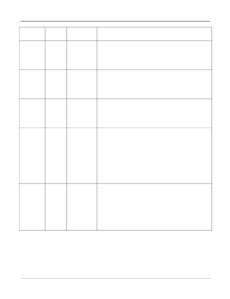
D12
107
OSC_EN
Oscillator Enable (5 V-Tolerant Input with Internal Pull-down)
If tied high, this pin indicates that there is a 20 MHz external
oscillator interfacing with the device. If tied low, there is no
oscillator and CKi will be used for master clock generation.
If the DPLL is activated, an external oscillator is required and this
pin
MUST
be tied high.
C12
149
OSCo
Oscillator Clock Output (3.3 V Output)
If OSC_EN = ‘1’, this pin should be connected to a 20 MHz crystal
(See Figure 23 on page 104) or left unconnected if a clock
oscillator is connected to OSCi pin under normal operation (See
Figure 24 on page 105).
If OSC_EN = 0, this pin
MUST
be left unconnected.
B14
148
OSCi
Oscillator Clock Input (3.3 V Input)
If OSC_EN = ‘1’, this pin should be connected to a 20 MHz crystal
(See Figure 23 on page 104) or to a clock oscillator under normal
operation (See Figure 24 on page 105).
If OSC_EN = 0, this pin
MUST
be driven high or low by connecting
either to V
DD_IO
or to ground.
DPLL Reference Inputs 0 to 3 (5 V-Tolerant Schmitt-Triggered
Inputs)
If the device is in Master mode, these input pins accept 8 kHz,
1.544 MHz, 2.048 MHz, 4.096 MHz, 8.192 MHz, 16.384 MHz or
19.44 MHz timing references independently. One of these inputs is
defined as the preferred or forced input reference for the DPLL.
The Reference Change Control Register (RCCR) selects the
control of the preferred reference.
These pins are ignored if the device is in slave mode unless
SLV_DPLLEN (bit 13) in the Control Register (CR) is set.
When these input pins are not in use, they
MUST
be driven high or
low by connecting either to V
DD_IO
or to ground.
Failure Indication for DPLL References 0 to 3 (5 V-Tolerant
Three-state Outputs)
These output pins are used to indicate input reference failure when
the device is in master mode.
If REF0 fails, REF_FAIL0 will be driven high.
If REF1 fails, REF_FAIL1 will be driven high.
If REF2 fails, REF_FAIL2 will be driven high.
If REF3 fails, REF_FAIL3 will be driven high.
If the device is in slave mode, these pins are driven low, unless
SLV_DPLLEN (bit 13) in the Control Register (CR) is set.
E9, D8, B8,
D7
161, 164,
166, 168
REF0 - 3
D9, E8, C8,
E7
159, 163,
165, 167
REF_FAIL0 - 3
PBGA Pin
Number
LQFP Pin
Number
Pin Name
Description
相關PDF資料 |
PDF描述 |
|---|---|
| ZL50018GAC | 2 K Digital Switch with Enhanced Stratum 3 DPLL |
| ZL50018QCC | 2 K Digital Switch with Enhanced Stratum 3 DPLL |
| ZL50019 | Enhanced 2 K Digital Switch with Stratum 4E DPLL |
| ZL50019GAC | Enhanced 2 K Digital Switch with Stratum 4E DPLL |
| ZL50019QCC | Enhanced 2 K Digital Switch with Stratum 4E DPLL |
相關代理商/技術參數 |
參數描述 |
|---|---|
| ZL50018_06 | 制造商:ZARLINK 制造商全稱:Zarlink Semiconductor Inc 功能描述:2 K Digital Switch with Enhanced Stratum 3 DPLL |
| ZL50018GAC | 制造商:Microsemi Corporation 功能描述:SWIT FABRIC 2K X 2K 1.8V/3.3V 256BGA - Trays 制造商:MICROSEMI CONSUMER MEDICAL PRODUCT GROUP 功能描述:IC TDM SWITCH 2K-CH ENH 256PBGA 制造商:Microsemi Corporation 功能描述:IC TDM SWITCH 2K-CH ENH 256PBGA |
| ZL50018GAG2 | 制造商:Microsemi Corporation 功能描述:SWIT FABRIC 2K X 2K 1.8V/3.3V 256BGA - Trays 制造商:MICROSEMI CONSUMER MEDICAL PRODUCT GROUP 功能描述:IC TDM SWITCH 2K-CH ENH 256PBGA 制造商:Microsemi Corporation 功能描述:IC TDM SWITCH 2K-CH ENH 256PBGA |
| ZL50018QCC | 制造商:Microsemi Corporation 功能描述:SWIT FABRIC 2K X 2K 1.8V/3.3V 256LQFP - Trays |
| ZL50018QCG1 | 制造商:Microsemi Corporation 功能描述:PB FREE 2K+ RATE CONVERSION AND S3 DPLL - Trays 制造商:MICROSEMI CONSUMER MEDICAL PRODUCT GROUP 功能描述:IC TDM SWITCH 2K-CH ENH 256LQFP |
發(fā)布緊急采購,3分鐘左右您將得到回復。