- 您現(xiàn)在的位置:買賣IC網(wǎng) > PDF目錄166216 > AM29LV256MH128EI (ADVANCED MICRO DEVICES INC) 16M X 16 FLASH 3V PROM, 120 ns, PDSO56 PDF資料下載
參數(shù)資料
| 型號: | AM29LV256MH128EI |
| 廠商: | ADVANCED MICRO DEVICES INC |
| 元件分類: | PROM |
| 英文描述: | 16M X 16 FLASH 3V PROM, 120 ns, PDSO56 |
| 封裝: | TSOP-56 |
| 文件頁數(shù): | 33/63頁 |
| 文件大小: | 1515K |
| 代理商: | AM29LV256MH128EI |
第1頁第2頁第3頁第4頁第5頁第6頁第7頁第8頁第9頁第10頁第11頁第12頁第13頁第14頁第15頁第16頁第17頁第18頁第19頁第20頁第21頁第22頁第23頁第24頁第25頁第26頁第27頁第28頁第29頁第30頁第31頁第32頁當前第33頁第34頁第35頁第36頁第37頁第38頁第39頁第40頁第41頁第42頁第43頁第44頁第45頁第46頁第47頁第48頁第49頁第50頁第51頁第52頁第53頁第54頁第55頁第56頁第57頁第58頁第59頁第60頁第61頁第62頁第63頁
September 9, 2002
Am29LV256M
39
A D VA NCE
I N FO RM ATIO N
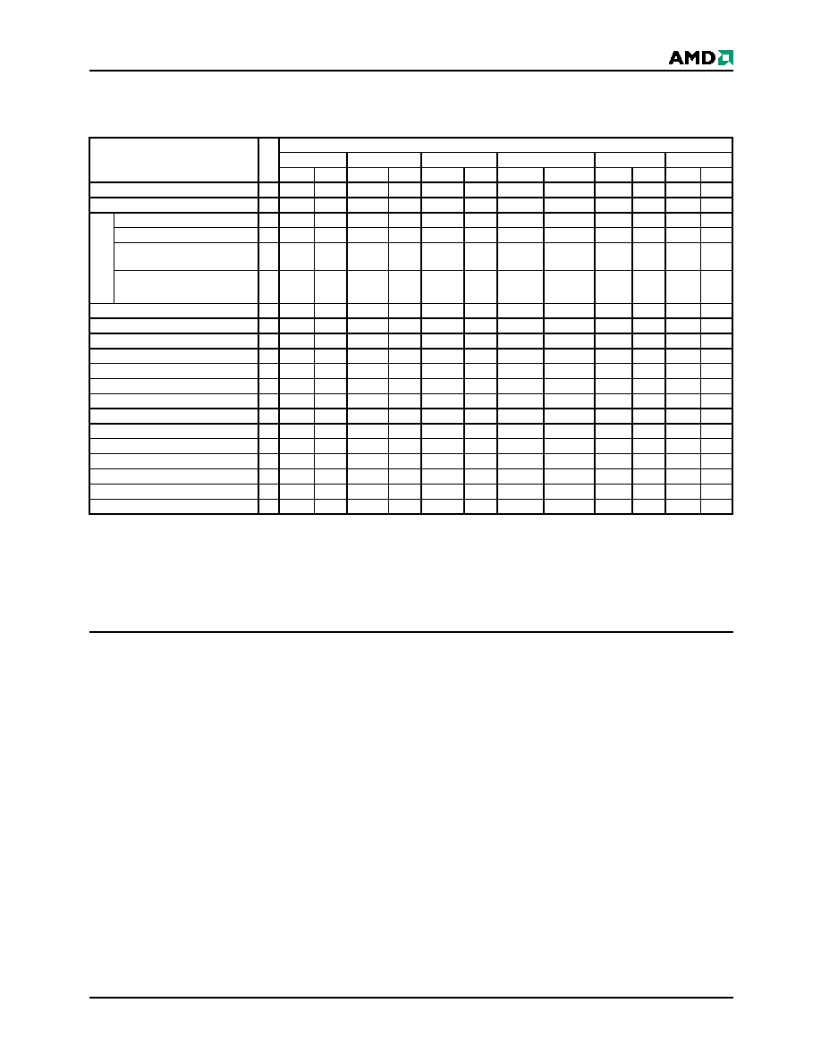
Command Definitions
Table 9.
Command Definitions (x16 Mode, BYTE# = V
IH)
Legend:
X = Don’t care
RA = Read Address of the memory location to be read.
RD = Read Data read from location RA during read operation.
PA = Program Address. Addresses latch on the falling edge of the WE#
or CE# pulse, whichever happens later.
PD = Program Data for location PA. Data latches on the rising edge of
WE# or CE# pulse, whichever happens first.
SA = Sector Address of sector to be verified (in autoselect mode) or
erased. Address bits A23–A15 uniquely select any sector.
WBL = Write Buffer Location. Address must be within the same write
buffer page as PA.
WC = Word Count. Number of write buffer locations to load minus 1.
Notes:
1.
See Table 1 for description of bus operations.
2.
All values are in hexadecimal.
3.
Except for the read cycle and the fourth cycle of the autoselect
command sequence, all bus cycles are write cycles.
4.
Data bits DQ15–DQ8 are don’t care in command sequences,
except for RD and PD.
5.
Unless otherwise noted, address bits A23–A11 are don’t cares.
6.
No unlock or command cycles required when device is in read
mode.
7.
The Reset command is required to return to the read mode (or to
the erase-suspend-read mode if previously in Erase Suspend)
when the device is in the autoselect mode, or if DQ5 goes high
while the device is providing status information.
8.
The fourth cycle of the autoselect command sequence is a read
cycle. Data bits DQ15–DQ8 are don’t care. See the Autoselect
Command Sequence section for more information.
9.
The device ID must be read in three cycles.
10. If WP# protects the highest address sector, the data is 98h for
factory locked and 18h for not factory locked. If WP# protects the
lowest address sector, the data is 88h for factory locked and 08h
for not factor locked.
11. The total number of cycles in the command sequence is
determined by the number of words written to the write buffer. The
maximum number of cycles in the command sequence is 21.
12. The data is 00h for an unprotected sector and 01h for a protected
sector.
13. Command sequence resets device for next command after
aborted write-to-buffer operation.
14. The Unlock Bypass command is required prior to the Unlock
Bypass Program command.
15. The Unlock Bypass Reset command is required to return to the
read mode when the device is in the unlock bypass mode.
16. The system may read and program in non-erasing sectors, or
enter the autoselect mode, when in the Erase Suspend mode.
The Erase Suspend command is valid only during a sector erase
operation.
17. The Erase Resume command is valid only during the Erase
Suspend mode.
18. Command is valid when device is ready to read array data or when
device is in autoselect mode.
Command
Sequence
C
y
cl
es
Bus Cycles (Notes 2–5)
First
Second
Third
Fourth
Fifth
Sixth
Addr
Data
Addr
Data
Addr
Data
Addr
Data
Addr
Data
Addr
Data
Read (Note 6)
1
RA
RD
Reset (Note 7)
1
XXX
F0
Auto
s
e
le
c
t(
Manufacturer ID
4
555
AA
2AA
55
555
90
X00
0001
Device ID (Note 9)
4
555
AA
2AA
55
555
90
X01
227E
X0E
2212
X0F
2201
SecSi
TM Sector Factory Protect
4
555
AA
2AA
55
555
90
X03
Sector Protect Verify (Note 12)
4
555
AA
2AA
55
555
90
(SA)X02
00/01
Enter SecSi Sector Region
3
555
AA
2AA
55
555
88
Exit SecSi Sector Region
4
555
AA
2AA
55
555
90
XXX
00
Program
4
555
AA
2AA
55
555
A0
PA
PD
Write to Buffer (Note 11)
3
555
AA
2AA
55
SA
25
SA
WC
PA
PD
WBL
PD
Program Buffer to Flash
1
SA
29
Write to Buffer Abort Reset (Note 13)
3
555
AA
2AA
55
555
F0
Unlock Bypass
3
555
AA
2AA
55
555
20
Unlock Bypass Program (Note 14)
2
XXX
A0
PA
PD
Unlock Bypass Reset (Note 15)
2
XXX
90
XXX
00
Chip Erase
6
555
AA
2AA
55
555
80
555
AA
2AA
55
555
10
Sector Erase
6
555
AA
2AA
55
555
80
555
AA
2AA
55
SA
30
Program/Erase Suspend (Note 16)
1
BA
B0
Program/Erase Resume (Note 17)
1
BA
30
CFI Query (Note 18)
1
55
98
相關(guān)PDF資料 |
PDF描述 |
|---|---|
| AM29LV256MH118REI | 16M X 16 FLASH 3V PROM, 110 ns, PDSO56 |
| AM29PDL127H83PCIN | 128 Megabit (8 M x 16-Bit) CMOS 3.0 Volt-only, Page Mode Simultaneous Read/Write Flash Memory with Enhanced VersatileIO Control |
| AM29PDL127H83VKIN | 128 Megabit (8 M x 16-Bit) CMOS 3.0 Volt-only, Page Mode Simultaneous Read/Write Flash Memory with Enhanced VersatileIO Control |
| AM29PDL127H85PCI | 128 Megabit (8 M x 16-Bit) CMOS 3.0 Volt-only, Page Mode Simultaneous Read/Write Flash Memory with Enhanced VersatileIO Control |
| AM29PDL127H85PCIN | 128 Megabit (8 M x 16-Bit) CMOS 3.0 Volt-only, Page Mode Simultaneous Read/Write Flash Memory with Enhanced VersatileIO Control |
相關(guān)代理商/技術(shù)參數(shù) |
參數(shù)描述 |
|---|---|
| AM29LV256MH94REI | 制造商:Spansion 功能描述:256M (32MX8/16MX16) 3V REG, MIRRORBIT, TSOP56, IND - Trays |
| AM29LV320DB120EI | 制造商:Spansion 功能描述:Flash Mem Parallel 3V/3.3V 32M-Bit 4M x 8/2M x 16 120ns 48-Pin TSOP |
| AM29LV320DB120WMI | 制造商:Spansion 功能描述:Flash Mem Parallel 3V/3.3V 32M-Bit 4M x 8/2M x 16 120ns 48-Pin FBGA |
| AM29LV320DB90EC | 制造商:Spansion 功能描述:Flash Mem Parallel 3V/3.3V 32M-Bit 4M x 8/2M x 16 90ns 48-Pin TSOP |
| AM29LV320DB90ED | 制造商:Spansion 功能描述:Flash Mem Parallel 3V/3.3V 32M-Bit 4M x 8/2M x 16 90ns 48-Pin TSOP |
發(fā)布緊急采購,3分鐘左右您將得到回復。