- 您現(xiàn)在的位置:買(mǎi)賣(mài)IC網(wǎng) > PDF目錄379668 > AN-937 (Electronic Theatre Controls, Inc.) Gate Drive Characteristics and Requirements for HEXFET PDF資料下載
參數(shù)資料
| 型號(hào): | AN-937 |
| 廠商: | Electronic Theatre Controls, Inc. |
| 英文描述: | Gate Drive Characteristics and Requirements for HEXFET |
| 中文描述: | 門(mén)驅(qū)動(dòng)器的特點(diǎn)及要求的HEXFET |
| 文件頁(yè)數(shù): | 19/21頁(yè) |
| 文件大小: | 418K |
| 代理商: | AN-937 |
第1頁(yè)第2頁(yè)第3頁(yè)第4頁(yè)第5頁(yè)第6頁(yè)第7頁(yè)第8頁(yè)第9頁(yè)第10頁(yè)第11頁(yè)第12頁(yè)第13頁(yè)第14頁(yè)第15頁(yè)第16頁(yè)第17頁(yè)第18頁(yè)當(dāng)前第19頁(yè)第20頁(yè)第21頁(yè)
AN-937 (v.Int)
9. SIMPLE AND INEXPENSIVE METHODS TO GENERATE ISOLATED
GATE DRIVE SUPPLIES
.
In several applications, dc-to-dc converters are used to power the MOS Gate Driver. Although the gate drive requires little
power, the noisy environment, the isolation voltage and creepage distance requirements and the high dv/dt between the primary
and secondary size make the design of the DC-to-DC converter somewhat complicated. Its key parameters are listed below:
OUTPUT VOLTAGE, CURRENT. The output voltage of the DC-to-DC converter is the sum of the positive and negative drive
voltage to the gate. The load current required from the DC-to-DC converter is the sum of the current consumption of the drive
circuit and the average drive current to the gate.
dv/dt CAPABILITY. When the DC-
DC converter powers a high side
switch, the secondary side of the
converter is connected to the output of
the power circuit. The rapid change of
high voltage at the output of power
circuit stresses the isolation of the
transformer and injects noise to the
primary side of the transformer.
Switching noise at the primary side
disturbs the operation of the converter
and the control circuit for the power
stage, causing false triggering and
shoot-through.
transformer
with
isolation,
appropriate
distances and low winding-to-
winding capacitance is required in this
application.
Therefore
high
a
voltage
creepage
SMALL SIZE. To reduce the interwinding capacitances the transformer must be made small. This implies operation at high
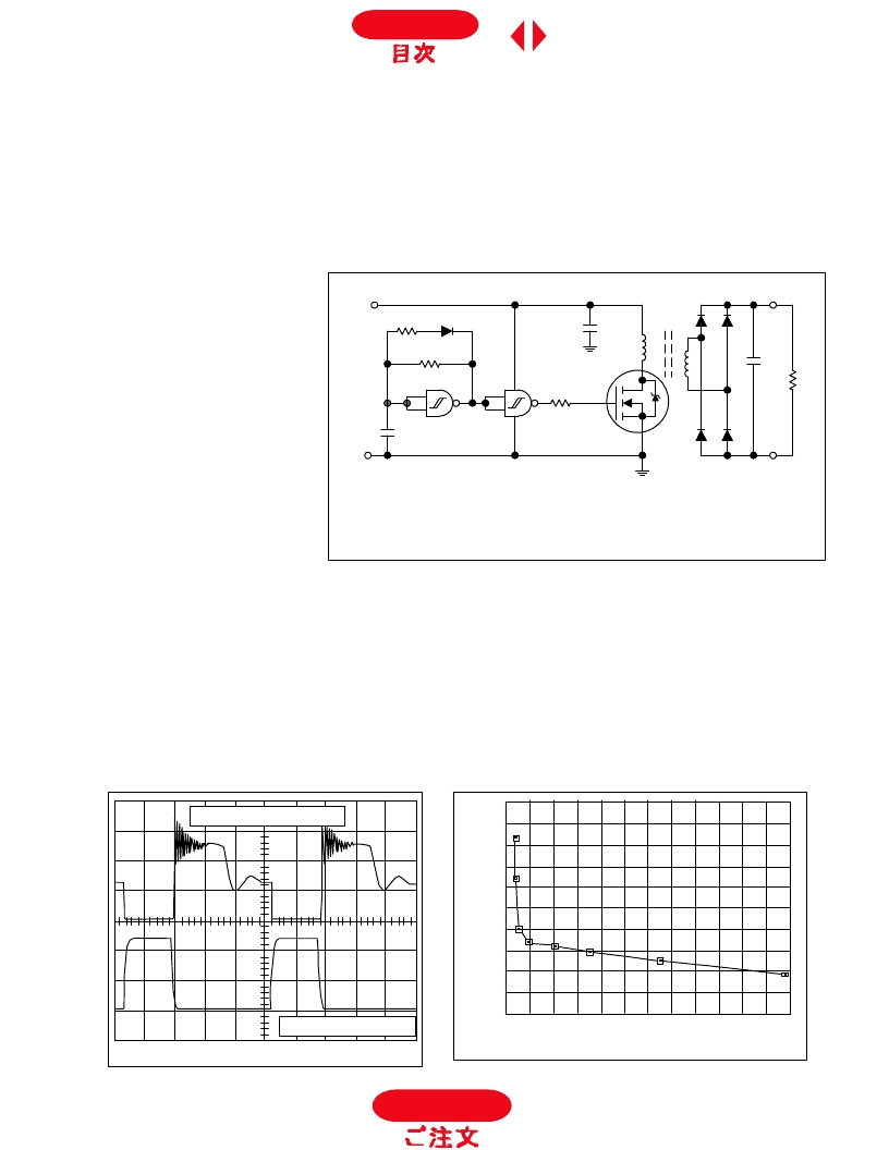
frequency. Small size and compact layout help reducing the EMI and RFI generated by the converter. Figure 33a shows a
forward converter made with two CD4093 gates to generate the clock and drive the MOSFET. Energy as transferred to the
secondary when the MOSFET is on, in about 33% of the cycle. When the MOSFET is off, the secondary winding is used to
demagnetize the transformer and transfer the magnetizing energy to the load, thus eliminating the need for a demagnetizing
winding. The switching waveforms are shown in Figure 33b. The ringing in the drain voltage during the fly-back period is due to
the loose coupling between the primary and the secondary windings. The load current vs. output voltage characteristic of the
circuit is shown in Figure 34. When the output current falls below 5 mA, the circuit works as flyback converter because the
demagnetizing current flows through the output. A minimum load of 5mA is required to limit the output voltage at 15V.
+12V
Figure 33a.
100 kHz Forward converter
13
12
11 100
1
μ
F
IRFD110
1N4148
12K
20K
5
6
4
CD4093
1n
12V
RTN
1
μ
F
T1
4X
IN4148
V
0
R
L
f = 100kHz
T1 TRANSFORMER: DORE: PHILIPS 240XT250-3EA2 TOROID
(OD = 0.75", Ae=0.148CM^2, AI=3000)
PRIMARY: 14 TURNS, AWG 30 TEFLON INSULATED WIRE
SECONDARY: 24 TURNS, AWG 30 TEFLON INSULATED WIRE
Gate voltage: 5V/div.
Drain voltage: 10V/div.
Horiz: 2
μ
s/div.
Figure 33b.
Waveforms associated with the
circuit in Figure 33a
35
30
25
20
15
10
0
20
40
60
80
100
120
Load current (mA)
O
Figure 34.
Load current vs. output voltage at 100 kHz,
Rout = 27.7 Ohms
To Order
Index
相關(guān)PDF資料 |
PDF描述 |
|---|---|
| AN1000-521P | AN0625-521P |
| AN0625-521P | AN0625-521P |
| AN0750-521P | AN0625-521P |
| AN0875-521P | AN0625-521P |
| AN1125-521P | AN0625-521P |
相關(guān)代理商/技術(shù)參數(shù) |
參數(shù)描述 |
|---|---|
| AN938-6 | 制造商: 功能描述: |
| AN939 | 制造商:MICROCHIP 制造商全稱:Microchip Technology 功能描述:Designing Energy Meters with the PIC16F873A |
| AN939-12D | 制造商: 功能描述: 制造商:undefined 功能描述: |
| AN93B06K | 制造商:Panasonic Industrial Company 功能描述:IC |
| AN93B06SCR | 制造商:PANASONIC 制造商全稱:Panasonic Semiconductor 功能描述:BROAD BAND VIDEO AMPLIFIER IC FOR CRT MONITOR |
發(fā)布緊急采購(gòu),3分鐘左右您將得到回復(fù)。