- 您現(xiàn)在的位置:買賣IC網(wǎng) > PDF目錄379668 > AN-937 (Electronic Theatre Controls, Inc.) Gate Drive Characteristics and Requirements for HEXFET PDF資料下載
參數(shù)資料
| 型號(hào): | AN-937 |
| 廠商: | Electronic Theatre Controls, Inc. |
| 英文描述: | Gate Drive Characteristics and Requirements for HEXFET |
| 中文描述: | 門驅(qū)動(dòng)器的特點(diǎn)及要求的HEXFET |
| 文件頁數(shù): | 21/21頁 |
| 文件大小: | 418K |
| 代理商: | AN-937 |
AN-937 (v.Int)
In the case of the MOSFET, there is the possibility that, for low current levels, the current flows through both MOSFET
channels, instead that one MOSFETs and diode, thereby achieving lower overall voltage drop. The MOSFET channel is a
bidirectional switch, that is, it can conduct current in the reverse direction.
If the voltage across the MOSFET
channel is less than the VF of the
intrinsic diode (which typically has a
higher VF than discrete diodes), then
the majority of the current will flow
through the MOSFET channel
instead of the intrinsic diode. The
gate drive for both the MOSFETs and
IGBTs must be referenced to the
common sources or emitters of the
devices. Since this node will be
swinging with the AC waveform, an
isolated drive is necessary. The PVI
can be used, as shown in Figure 40.
11. RESONANT GATE DRIVE TECHNIQUES
As indicated in Section 14, gate drive losses in hard switching are
equal to Qgs x Vgs x f. An IRF630 operated at 10 Mhz with a
gate voltage of 12 V would have
gate drive losses
of 3.6 W,
independent from the value of the gate drive resistor. Clearly, to
achieve hard switching at this frequency, the resistance of the gate
drive circuit is limited to whatever is associated with the internal
impedance of the driver and with the gate structure of the device
itself. Furthermore, the stray inductance of the gate drive circuit
must be limited to tens of nH. The design and layout of such a
circuit is not an easy task.
An alternative method to drive the gate in such an application is
to design a resonant circuit that makes use of the gate capacitance
and stray inductance as its reactive components, adding whatever
inductance is necessary to achieve resonance at the desired
frequency. This method can reduce the peak of the gate drive
current and losses in half, while simplifying the design of the gate
drive circuit itself. Since the gate charge is not dissipated at every
switching transition, but stored in a reactive component, the gate
drive losses are proportional to the resistance of the gate drive
circuit, rather than being independent from it. More information
on this gate drive method can be found in an article by El-
Hamamsy: Design of High-Efficiency RF Class-D Power
Amplifier and in references at the end of this article (IEEE
Transactions on Power Electronics, May 1994, page 297).
Related Topics
MOS-Gate Driver Ics
Transformer drive with wide duty cycle capability
Gate Charge
Three-phase MOS-Gate Driver
Photovoltaic Isolators (PVI)
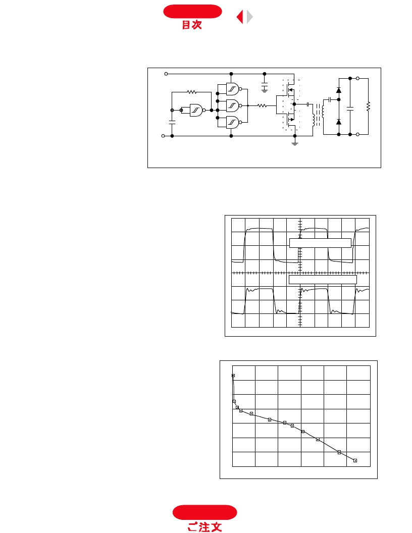
+12V
Figure 37a.
500 kHz Forward converter
13
12
11
100
1
μ
F
10K
5
6
4
CD4093
220p
12V
RTN
1
μ
F
T1
1N4148
V
0
R
L
f = 500kHz
T1: CORE: PHILIPS 266CT125-3E2A (od=0.375", Ae=0.072CM^2, AL=2135
PRIMARY: 4T, AWG 30, SECONDARY: 7T, AWG30
9
8
10
1
2
3
14
7
7, 8
2
4
5, 6
1
3
7T
1N4148
100nF
100nF
2T
IRF7307
Buffer input: 5V/div.
Buffer Output: 5V/div.
Horiz.: 500ns/div
Figure 37b.
Waveforms associated with the circuit in Figure 37a
20
19
18
17
16
15
14
13
0
10
20
30
40
50
60
Figure 38.
Load current vs. output voltage,
Rout=27.7 Ohms
To Order
Index
相關(guān)PDF資料 |
PDF描述 |
|---|---|
| AN1000-521P | AN0625-521P |
| AN0625-521P | AN0625-521P |
| AN0750-521P | AN0625-521P |
| AN0875-521P | AN0625-521P |
| AN1125-521P | AN0625-521P |
相關(guān)代理商/技術(shù)參數(shù) |
參數(shù)描述 |
|---|---|
| AN938-6 | 制造商: 功能描述: |
| AN939 | 制造商:MICROCHIP 制造商全稱:Microchip Technology 功能描述:Designing Energy Meters with the PIC16F873A |
| AN939-12D | 制造商: 功能描述: 制造商:undefined 功能描述: |
| AN93B06K | 制造商:Panasonic Industrial Company 功能描述:IC |
| AN93B06SCR | 制造商:PANASONIC 制造商全稱:Panasonic Semiconductor 功能描述:BROAD BAND VIDEO AMPLIFIER IC FOR CRT MONITOR |
發(fā)布緊急采購,3分鐘左右您將得到回復(fù)。