- 您現(xiàn)在的位置:買賣IC網(wǎng) > PDF目錄385432 > HYB18L256160B (QIMONDA) DRAMs for Mobile Applications 256-Mbit Mobile-RAM PDF資料下載
參數(shù)資料
| 型號(hào): | HYB18L256160B |
| 廠商: | QIMONDA |
| 英文描述: | DRAMs for Mobile Applications 256-Mbit Mobile-RAM |
| 中文描述: | DRAM的針對(duì)移動(dòng)應(yīng)用256兆移動(dòng)RAM |
| 文件頁數(shù): | 51/58頁 |
| 文件大小: | 1766K |
| 代理商: | HYB18L256160B |
第1頁第2頁第3頁第4頁第5頁第6頁第7頁第8頁第9頁第10頁第11頁第12頁第13頁第14頁第15頁第16頁第17頁第18頁第19頁第20頁第21頁第22頁第23頁第24頁第25頁第26頁第27頁第28頁第29頁第30頁第31頁第32頁第33頁第34頁第35頁第36頁第37頁第38頁第39頁第40頁第41頁第42頁第43頁第44頁第45頁第46頁第47頁第48頁第49頁第50頁當(dāng)前第51頁第52頁第53頁第54頁第55頁第56頁第57頁第58頁
Data Sheet
Rev. 1.73, 2006-09
01302004-CZ2R-J9SE
51
HY[B/E]18L256160B[C/F]L-7.5
256-Mbit Mobile-RAM
3.3
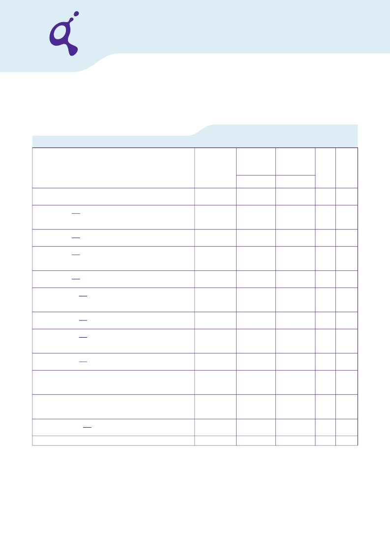
Operating Currents
TABLE 27
Maximum Operating Currents
Parameter & Test Conditions
Symbol
Values for
HY[B/E]...
160B[C/F]
Values for
HYE...
160B[C/F]L
Unit
Note
1)
1) 0
°
C
≤
T
C
≤
70
°
C (comm.); -25
°
C
≤
T
C
≤
85
°
C (ext.);
V
DD
=
V
DDQ
= 1.65V to 1.95V;
Recommended Operating Conditions unless otherwise noted
2) These values are measured with
t
CK
= 7.5 ns
3) All parameters are measured with no output loads.
- 7.5
- 7.5
Operating current:
one bank: active / read / precharge, BL = 1,
t
RC
=
t
RCmin
Precharge power-down standby current:
all banks idle, CS
≥
V
IHmin
, CKE
≤
V
ILmax
,
inputs changing once every two clock cycles
Precharge power-down standby current with clock stop:
all banks idle, CS
≥
V
IHmin
, CKE
≤
V
ILmax
, all inputs stable
Precharge non power-down standby current:
all banks idle, CS
≥
V
IHmin
, CKE
≥
V
IHmin
,
inputs changing once every two clock cycles
Precharge non power-down standby current with clock stop:
all banks idle, CS
≥
V
IHmin
, CKE
≥
V
IHmin
, all inputs stable
Active power-down standby current:
one bank active, CS
≥
V
IHmin
, CKE
≤
V
ILmax
,
inputs changing once every two clock cycles
Active power-down standby current with clock stop:
one bank active, CS
≥
V
IHmin
, CKE
≤
V
ILmax
, all inputs stable
Active non power-down standby current:
one bank active, CS
≥
V
IHmin
, CKE
≥
V
IHmin
,
inputs changing once every two clock cycles
Active non power-down standby current with clock stop:
one bank active, CS
≥
V
IHmin
, CKE
≥
V
IHmin
, all inputs stable
Operating burst read current:
all banks active; continuous burst read,
inputs changing once every two clock cycles
Auto-Refresh current:
t
RC
=
t
RCmin
, “burst refresh”,
inputs changing once every two clock cycles
Self Refresh current:
self refresh mode, CS
≥
V
IHmin
, CKE
≤
V
ILmax
, all inputs stable
Deep Power Down current
I
DD1
60
60
mA
2)3)
I
DD2P
0.6
0.4
mA
2)
I
DD2PS
0.5
0.35
mA
–
I
DD2N
13
13
mA
2)
I
DD2NS
1.0
1.0
mA
–
I
DD3P
1.0
1.0
mA
2)
I
DD3PS
0.75
0.5
mA
–
I
DD3N
15
15
mA
2)
I
DD3NS
1.5
1.5
mA
–
I
DD4
45
45
mA
2)3)
I
DD5
90
90
mA
2)
I
DD6
See
Table 28
–
I
DD7
20
20
μ
A
–
相關(guān)PDF資料 |
PDF描述 |
|---|---|
| HYMP112S64LMP8-C4 | DDR2 SDRAM SO-DIMM |
| HYMP112S64LMP8-C5 | DDR2 SDRAM SO-DIMM |
| HYMP112S64LMP8-E3 | BNC FEMALE TO RCA MALE COUPLER |
| HYMP112S64LMP8-E4 | DDR2 SDRAM SO-DIMM |
| HYMP112S64MP8 | SHIELDED, RJ45 TO DB25 ADP, P |
相關(guān)代理商/技術(shù)參數(shù) |
參數(shù)描述 |
|---|---|
| HYB18L256160BC-7.5 | 制造商:INFINEON 制造商全稱:Infineon Technologies AG 功能描述:BJAWBMSpecialty DRAMs Mobile-RAM |
| HYB18L256160BC-75 | 制造商:INFINEON 制造商全稱:Infineon Technologies AG 功能描述:DRAMs for Mobile Applications |
| HYB18L256160BCL-7.5 | 制造商:QIMONDA 制造商全稱:QIMONDA 功能描述:DRAMs for Mobile Applications 256-Mbit Mobile-RAM |
| HYB18L256160BCX-7.5 | 制造商:QIMONDA 制造商全稱:QIMONDA 功能描述:DRAMs for Mobile Applications 256-Mbit Mobile-RAM |
| HYB18L256160BF | 制造商:INFINEON 制造商全稱:Infineon Technologies AG 功能描述:DRAMs for Mobile Applications |
發(fā)布緊急采購,3分鐘左右您將得到回復(fù)。