- 您現(xiàn)在的位置:買賣IC網(wǎng) > PDF目錄377496 > INTEL486 GX (Intel Corp.) Emedded Ultra-Low Power INTEL486 GX Processor(嵌入式超低能量處理器) PDF資料下載
參數(shù)資料
| 型號: | INTEL486 GX |
| 廠商: | Intel Corp. |
| 英文描述: | Emedded Ultra-Low Power INTEL486 GX Processor(嵌入式超低能量處理器) |
| 中文描述: | Emedded超低功耗英特爾486 GX處理器(嵌入式超低能量處理器) |
| 文件頁數(shù): | 21/48頁 |
| 文件大?。?/td> | 409K |
| 代理商: | INTEL486 GX |
第1頁第2頁第3頁第4頁第5頁第6頁第7頁第8頁第9頁第10頁第11頁第12頁第13頁第14頁第15頁第16頁第17頁第18頁第19頁第20頁當(dāng)前第21頁第22頁第23頁第24頁第25頁第26頁第27頁第28頁第29頁第30頁第31頁第32頁第33頁第34頁第35頁第36頁第37頁第38頁第39頁第40頁第41頁第42頁第43頁第44頁第45頁第46頁第47頁第48頁
Embedded Ultra-Low Power Intel486 GX Processor
17
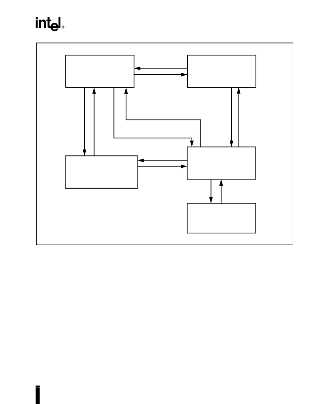
Figure 4. Stop Clock State Diagram with Typical Power Consumption Values
4 Auto HALT
Power Down State
CLK Running
40 - 85 mWatts
5 Stop Clock Snoop State
One Clock PowerUp
Perform Cache Invalidation
1 Normal State
Normal Execution
2 Stop Grant State
CLK Running
40 - 85 mWatts
3 Stop Clock State
Internal Powerdown
CLK Stopped
~ 60 μWatts
EADS#
STPCLK#
deasserted
Stop CLK
Start CLK
plus DDL Startup
Latency
STPCLK# asserted
and Stop Grant bus
cycle generated
STPCLK# asserted and
Stop Grant bus cycle generated
STPCLK# deasserted and
HALT bus cycle generated
HALT asserted and
HALT bus cycle
generated
INTR, NMI, SMI#
RESET, SRESET
EADS#
4.3
Level-Keeper Circuits
To obtain the lowest possible power consumption
during the Stop Grant and Stop Clock states, system
designers must ensure that:
input signals with pull-up resistors are not driven
LOW
input signals with pull-down resistors are not
driven HIGH
See Table 8, Input Pins (pg. 14) for the list of signals
with internal pull-up and pull-down resistors.
All other input pins except A31-A4, D15-D0, DP1,
and DP0 must be driven to the power supply rails to
ensure lowest possible current consumption.
During the Stop Grant and Stop Clock states, most
processor output signals maintain their previous
condition, which is the level they held when entering
the Stop Grant state. In response to HOLD driven
active during the Stop Grant state when the CLK
input is running, the embedded ULP Intel486 GX
processor generates HLDA and floats all output and
input/output signals which are floated during the
HOLD/HLDA state. When HOLD is deasserted,
processor signals which maintain their previous state
return to the state they were in prior to the
HOLD/HLDA sequence.
The data bus (D15-D0) and parity bits also maintain
their previous states during the Stop Grant and Stop
Clock states, but do so differently, as described in
the following paragraphs.
相關(guān)PDF資料 |
PDF描述 |
|---|---|
| INTEL486 SX | Emedded Ultra-Low Power INTEL486 SX Processor(嵌入式超低能量處理器) |
| INTEL82801 | 82801AB (ICH0) I/O Controller Hub |
| INTEL82802AB | Firmware Hub (FWH) |
| INTELDX2 | High-Performance 32-Bit Embedded Processor(高性能32位嵌入式處理器) |
| INTELDX4 | Embedded Write-Back Enhanced Processor(32位回復(fù)嵌入式增強(qiáng)型處理器) |
相關(guān)代理商/技術(shù)參數(shù) |
參數(shù)描述 |
|---|---|
| INTEL740 | 制造商:未知廠家 制造商全稱:未知廠家 功能描述:64-Bit Graphics (GUI) Accelerator |
| INTEL82801 | 制造商:INTEL 制造商全稱:Intel Corporation 功能描述:82801AB (ICH0) I/O Controller Hub |
| INTEL82802AB | 制造商:INTEL 制造商全稱:Intel Corporation 功能描述:Firmware Hub (FWH) |
| INTELLIGENT CHARGER + 4AA | 制造商:Energizer 功能描述:Bulk |
| INTELLI-INCH-LR-STARTER K | 制造商:ALL MOTION 功能描述:Intelli-Inch Stepper & Controller Starter Kit |
發(fā)布緊急采購,3分鐘左右您將得到回復(fù)。