- 您現(xiàn)在的位置:買賣IC網(wǎng) > PDF目錄224103 > K7R323682 (SAMSUNG SEMICONDUCTOR CO. LTD.) 1Mx36 & 2Mx18 & 4Mx9 QDRTM II b2 SRAM PDF資料下載
參數(shù)資料
| 型號: | K7R323682 |
| 廠商: | SAMSUNG SEMICONDUCTOR CO. LTD. |
| 英文描述: | 1Mx36 & 2Mx18 & 4Mx9 QDRTM II b2 SRAM |
| 中文描述: | 1Mx36 |
| 文件頁數(shù): | 2/19頁 |
| 文件大?。?/td> | 201K |
| 代理商: | K7R323682 |
1Mx36 & 2Mx18 & 4Mx9 QDRTM II b2 SRAM
- 10 -
Rev 2.0
Dec. 2003
K7R323682M
K7R321882M
K7R320982M
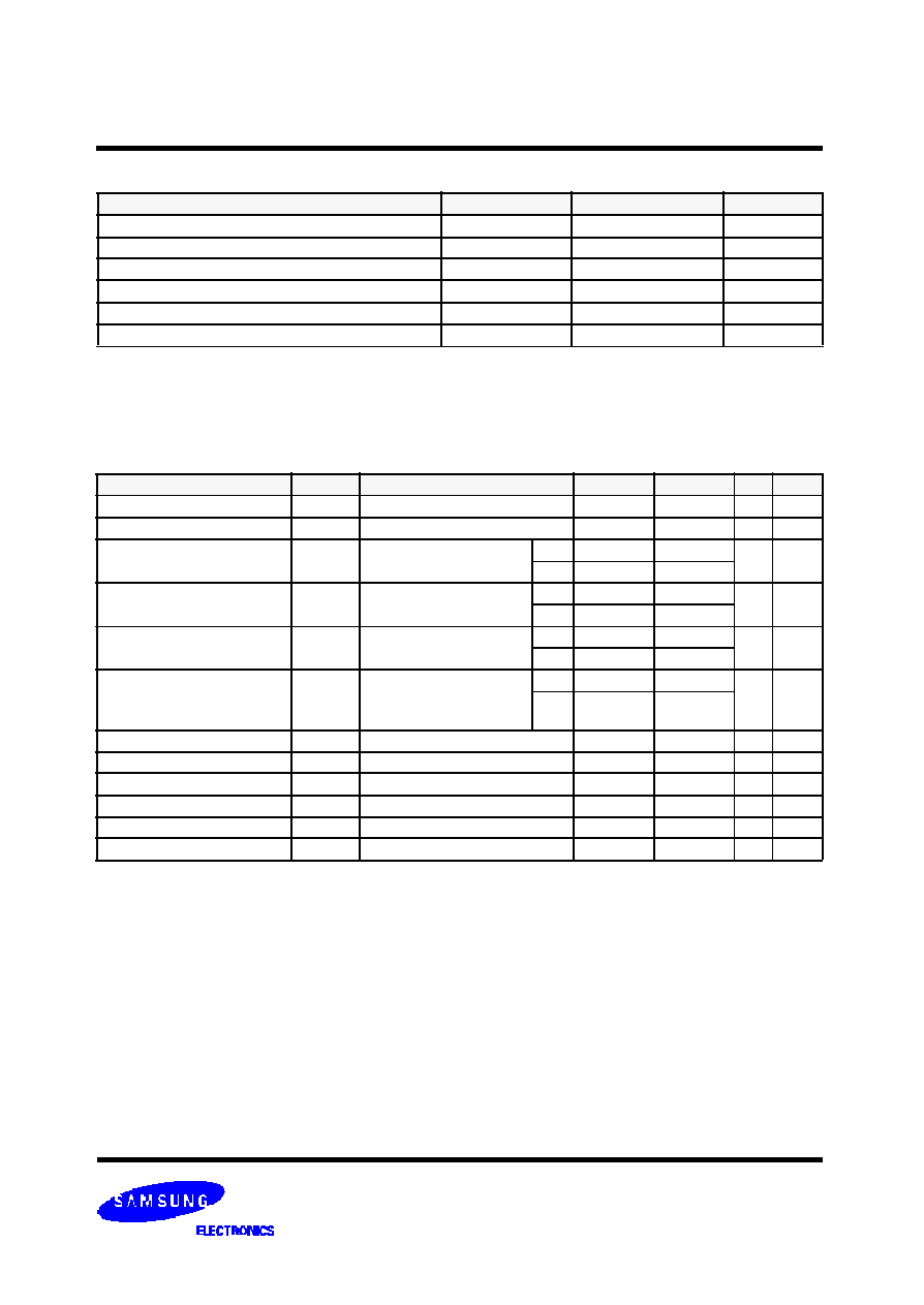
DC ELECTRICAL CHARACTERISTICS(VDD=1.8V
±0.1V, TA=0°C to +70°C)
Notes: 1. Minimum cycle. IOUT=0mA.
2. |IOH|=(VDDQ/2)/(RQ/5)
±15% for 175 ≤ RQ ≤ 350.
3. |IOL|=(VDDQ/2)/(RQ/5)
±15% for 175 ≤ RQ ≤ 350.
4. Minimum Impedance Mode when ZQ pin is connected to VDDQ .
5. Operating current is calculated with 50% read cycles and 50% write cycles.
6. Standby Current is only after all pending read and write burst opeactions are completed.
7. Programmable Impedance Mode.
8. These are DC test criteria. DC design criteria is V REF
±50mV. The AC VIH/VIL levels are defined separately for measuring timing parameters.
9. V IL (Min)DC=
-0.3V, VIL (Min)AC=-1.5V(pulse width
≤ 3ns).
10. VIH (Max)DC=
VDDQ+0.3, V IH (Max)AC=VDDQ+0.85V(pulse width
≤ 3ns).
PARAMETER
SYMBOL
TEST CONDITIONS
MIN
MAX
UNIT NOTES
Input Leakage Current
IIL
VDD=Max ; VIN=V SS to VDDQ
-2
+2
A
Output Leakage Current
IOL
Output Disabled,
-2
+2
A
Operating Current (x36): DDR
ICC
VDD=Max , IOUT=0mA
Cycle Time
≥ tKHKH Min
-20
-
870
mA
1,5
-16
-
740
Operating Current (x18): DDR
ICC
VDD=Max , IOUT=0mA
Cycle Time
≥ tKHKH Min
-20
-
760
mA
1,5
-16
-
650
Operating Current ( x9): DDR
ICC
VDD=Max , IOUT=0mA
Cycle Time
≥ tKHKH Min
-20
-
720
mA
1,5
-16
-
620
Standby Current(NOP): DDR
ISB1
Device deselected, I OUT=0mA,
f=Max,
All Inputs
≤0.2V or ≥ VDD-0.2V
-20
-
300
mA
1,6
-16
-
270
Output High Voltage
VOH1
VDDQ/2-0.12 VDDQ/2+0.12
V
2,7
Output Low Voltage
VOL1
VDDQ/2-0.12 VDDQ/2+0.12
V
3,7
Output High Voltage
VOH2
IOH=-1.0mA
VDDQ-0.2
VDDQ
V
4
Output Low Voltage
VOL2
IOL=1.0mA
VSS
0.2
V
4
Input Low Voltage
VIL
-0.3
VREF-0.1
V
8,9
Input High Voltage
VIH
VREF+0.1
VDDQ+0.3
V
8,10
ABSOLUTE MAXIMUM RATINGS*
*Note: 1. Stresses greater than those listed under "Absolute Maximum Ratings" may cause permanent damage to the device. This is a stress rating
only and functional operation of the device at these or any other conditions above those indicated in the operati ng sections of this specification
is not implied. Exposure to absolute maximum rating conditions for extended periods may affect reliability.
2. VDDQ must not exceed VDD during normal operation.
PARAMETER
SYMBOL
RATING
UNIT
Voltage on VDD Supply Relative to VSS
VDD
-0.5 to 2.9
V
Voltage on VDDQ Supply Relative to VSS
VDDQ
-0.5 to V DD
V
Voltage on Input Pin Relative to VSS
V IN
-0.5 to VDD+0.3
V
Storage Temperature
TSTG
-65 to 150
°C
Operating Temperature
TOPR
0 to 70
°C
Storage Temperature Range Under Bias
TBIAS
-10 to 85
°C
相關PDF資料 |
PDF描述 |
|---|---|
| K971 | 85.05 mm2, COPPER ALLOY, TIN FINISH, RING TERMINAL |
| K972 | 85.05 mm2, COPPER ALLOY, TIN FINISH, RING TERMINAL |
| K973 | 85.05 mm2, COPPER ALLOY, TIN FINISH, RING TERMINAL |
| KBJ402G | 4 A, 200 V, SILICON, BRIDGE RECTIFIER DIODE |
| KBPC3508W | 35 A, 800 V, SILICON, BRIDGE RECTIFIER DIODE |
相關代理商/技術參數(shù) |
參數(shù)描述 |
|---|---|
| K7R323682C | 制造商:SAMSUNG 制造商全稱:Samsung semiconductor 功能描述:1Mx36 & 2Mx18 & 4Mx9 QDR II b2 SRAM |
| K7R323682C-EC25000 | 制造商:Samsung SDI 功能描述: |
| K7R323682C-FC16000 | 制造商:Samsung 功能描述:32M 32MSYNC QUAD DATA RATE II X36 FBGA - Trays |
| K7R323682C-FC20 | 制造商:SAMSUNG 制造商全稱:Samsung semiconductor 功能描述:1Mx36 & 2Mx18 & 4Mx9 QDR II b2 SRAM |
| K7R323682C-FC25 | 制造商:SAMSUNG 制造商全稱:Samsung semiconductor 功能描述:1Mx36 & 2Mx18 & 4Mx9 QDR II b2 SRAM |
發(fā)布緊急采購,3分鐘左右您將得到回復。