- 您現(xiàn)在的位置:買賣IC網(wǎng) > PDF目錄224103 > K7R323682 (SAMSUNG SEMICONDUCTOR CO. LTD.) 1Mx36 & 2Mx18 & 4Mx9 QDRTM II b2 SRAM PDF資料下載
參數(shù)資料
| 型號: | K7R323682 |
| 廠商: | SAMSUNG SEMICONDUCTOR CO. LTD. |
| 英文描述: | 1Mx36 & 2Mx18 & 4Mx9 QDRTM II b2 SRAM |
| 中文描述: | 1Mx36 |
| 文件頁數(shù): | 8/19頁 |
| 文件大小: | 201K |
| 代理商: | K7R323682 |
1Mx36 & 2Mx18 & 4Mx9 QDRTM II b2 SRAM
- 16 -
Rev 2.0
Dec. 2003
K7R323682M
K7R321882M
K7R320982M
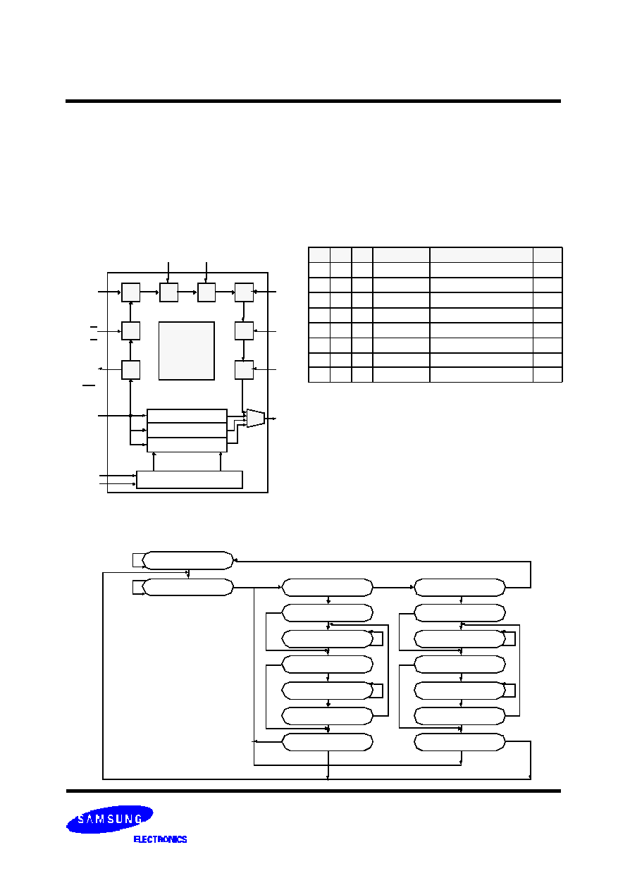
IEEE 1149.1 TEST ACCESS PORT AND BOUNDARY SCAN-JTAG
This part contains an IEEE standard 1149.1 Compatible Test Access Port(TAP). The package pads are monitored by the Serial Scan
circuitry when in test mode. This is to support connectivity testing during manufacturing and system diagnostics. Internal data is not
driven out of the SRAM under JTAG control. In conformance with IEEE 1149.1, the SRAM contains a TAP controller, Instruction Reg-
ister, Bypass Register and ID register. The TAP controller has a standard 16-state machine that resets internally upon power-up,
therefore, TRST signal is not required. It is possible to use this device without utilizing the TAP. To disable the TAP controller without
interfacing with normal operation of the SRAM, TCK must be tied to VSS to preclude mid level input. TMS and TDI are designed so an
undriven input will produce a response identical to the application of a logic 1, and may be left unconnected. But they may also be
tied to VDD through a resistor. TDO should be left unconnected.
TAP Controller State Diagram
JTAG Block Diagram
Test Logic Reset
Run Test Idle
0
1
0
1
0
1
0
1
0
1
0
Select DR
Capture DR
Shift DR
Exit1 DR
Pause DR
Exit2 DR
Update DR
Select IR
Capture IR
Shift IR
Exit1 IR
Pause IR
Exit2 IR
Update IR
1
JTAG Instruction Coding
NOTE :
1. Places DQs in Hi-Z in order to sample all input data regardless of other
SRAM inputs. This instruction is not IEEE 1149.1 compliant.
2. Places DQs in Hi-Z in order to sample all input data regardless of other
SRAM inputs.
3. TDI is sampled as an input to the first ID register to allow for the serial shift
of the external TDI data.
4. Bypass register is initiated to V SS when BYPASS instruction is invoked. The
Bypass Register also holds serially loaded TDI when exiting the Shift DR
states.
5. SAMPLE instruction dose not places DQs in Hi-Z.
6. This instruction is reserved for future use.
IR2
IR1
IR0
Instruction
TDO Output
Notes
0
EXTEST
Boundary Scan Register
1
0
1
IDCODE
Identification Register
3
0
1
0
SAMPLE-Z
Boundary Scan Register
2
0
1
RESERVED
Do Not Use
6
1
0
SAMPLE
Boundary Scan Register
5
1
0
1
RESERVED
Do Not Use
6
1
0
RESERVED
Do Not Use
6
1
BYPASS
Bypass Register
4
SRAM
CORE
BYPASS Reg.
Identification Reg.
Instruction Reg.
Control Signals
TAP Controller
TDO
TDI
TMS
TCK
CQ
K,K
C,C
A,D
Q
CQ
相關(guān)PDF資料 |
PDF描述 |
|---|---|
| K971 | 85.05 mm2, COPPER ALLOY, TIN FINISH, RING TERMINAL |
| K972 | 85.05 mm2, COPPER ALLOY, TIN FINISH, RING TERMINAL |
| K973 | 85.05 mm2, COPPER ALLOY, TIN FINISH, RING TERMINAL |
| KBJ402G | 4 A, 200 V, SILICON, BRIDGE RECTIFIER DIODE |
| KBPC3508W | 35 A, 800 V, SILICON, BRIDGE RECTIFIER DIODE |
相關(guān)代理商/技術(shù)參數(shù) |
參數(shù)描述 |
|---|---|
| K7R323682C | 制造商:SAMSUNG 制造商全稱:Samsung semiconductor 功能描述:1Mx36 & 2Mx18 & 4Mx9 QDR II b2 SRAM |
| K7R323682C-EC25000 | 制造商:Samsung SDI 功能描述: |
| K7R323682C-FC16000 | 制造商:Samsung 功能描述:32M 32MSYNC QUAD DATA RATE II X36 FBGA - Trays |
| K7R323682C-FC20 | 制造商:SAMSUNG 制造商全稱:Samsung semiconductor 功能描述:1Mx36 & 2Mx18 & 4Mx9 QDR II b2 SRAM |
| K7R323682C-FC25 | 制造商:SAMSUNG 制造商全稱:Samsung semiconductor 功能描述:1Mx36 & 2Mx18 & 4Mx9 QDR II b2 SRAM |
發(fā)布緊急采購,3分鐘左右您將得到回復(fù)。