- 您現(xiàn)在的位置:買賣IC網(wǎng) > PDF目錄224506 > MT55L256L32FT-12 256K X 32 ZBT SRAM, 9 ns, PQFP100 PDF資料下載
參數(shù)資料
| 型號: | MT55L256L32FT-12 |
| 元件分類: | SRAM |
| 英文描述: | 256K X 32 ZBT SRAM, 9 ns, PQFP100 |
| 封裝: | PLASTIC, TQFP-100 |
| 文件頁數(shù): | 10/25頁 |
| 文件大小: | 300K |
| 代理商: | MT55L256L32FT-12 |
18
8Mb: 512K x 18, 256K x 32/36 Flow-Through ZBT SRAM
Micron Technology, Inc., reserves the right to change products or specifications without notice.
MT55L512L18F_C.p65 – Rev. 2/02
2002, Micron Technology, Inc.
8Mb: 512K x 18, 256K x 32/36
FLOW-THROUGH ZBT SRAM
NOTE: 1. This parameter is sampled.
2. OE# can be considered a “ Don’t Care” during WRITEs; however, controlling OE# can help fine-tune a system for
turnaround timing.
3. Test conditions as specified with output loading as shown in Figure 1 for 3.3V I/O (VDDQ = +3.3V ±0.165V) and
Figure 3 for 2.5V I/O (VDDQ = +2.5V +0.4V/-0.125V).
4. A WRITE cycle is defined by R/W# LOW having been registered into the device at ADV/LD# LOW. A READ cycle is
defined by R/W# HIGH with ADV/LD# LOW. Both cases must meet setup and hold times.
5. Measured as HIGH above VIH and LOW below VIL.
6. Refer to Technical Note TN-55-01, “ Designing with ZBT SRAMs,” for a more thorough discussion on these parameters.
7. This parameter is sampled.
8. This parameter is measured with output loading as shown in Figure 2 for 3.3V I/O and Figure 4 for 2.5V I/O.
9. Transition is measured ±200mV from steady state voltage.
10. This is a synchronous device. All addresses must meet the specified setup and hold times for all rising edges of CLK
when they are being registered into the device. All other synchronous inputs must meet the setup and hold times with
stable logic levels for all rising edges of clock (CLK) when the chip is enabled. Chip enable must be valid at each rising
edge of CLK when ADV/LD# is LOW to remain enabled.
11. Preliminary package data.
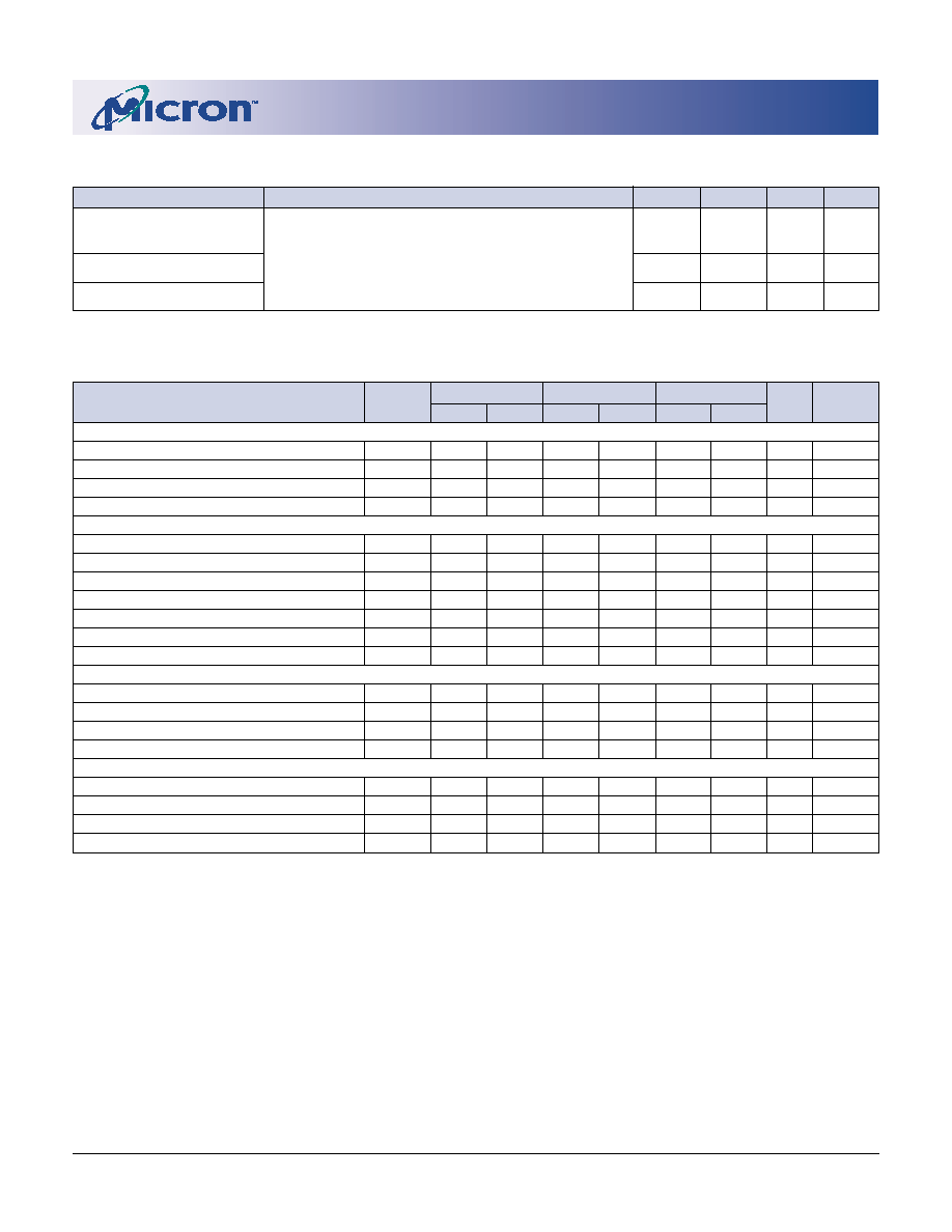
AC ELECTRICAL CHARACTERISTICS
(Notes 2, 3, 4) (0° C
≤ T
A ≤ +70° C; VDD = +3.3V ±0.165V unless otherwise noted)
-10
-11
-12
DESCRIPTION
SYMBOL
MIN
MAX
MIN
MAX
MIN
MAX
UNITS
NOTES
Clock
Clock cycle time
tKHKH
10
11
12
ns
Clock frequency
fKF
100
90
83
MHz
Clock HIGH time
tKHKL
2.5
3.0
ns
5
Clock LOW time
tKLKH
2.5
3.0
ns
5
Output Times
Clock to output valid
tKHQV
7.5
8.5
9.0
ns
Clock to output invalid
tKHQX
3.0
ns
6
Clock to output in Low-Z
tKHQX1
3.0
ns
6, 7, 8, 9
Clock to output in High-Z
tKHQZ
5.0
ns
6, 7, 8, 9
OE# to output valid
tGLQV
5.0
ns
2
OE# to output in Low-Z
tGLQX
0
ns
6, 7, 8, 9
OE# to output in High-Z
tGHQZ
5.0
ns
6, 7, 8, 9
Setup Times
Address
tAVKH
2.0
2.2
2.5
ns
10
Clock enable (CKE#)
tEVKH
2.0
2.2
2.5
ns
10
Control signals
tCVKH
2.0
2.2
2.5
ns
10
Data-in
tDVKH
2.0
2.2
2.5
ns
10
Hold Times
Address
tKHAX
0.5
ns
10
Clock enable (CKE#)
tKHEX
0.5
ns
10
Control signals
tKHCX
0.5
ns
10
Data-in
tKHDX
0.5
ns
10
FBGA THERMAL RESISTANCE
DESCRIPTION
CONDITIONS
SYMBOL
TYP
UNITS NOTES
Junction to Ambient
Test conditions follow standard test methods
θ
JA
40
° C/W
1, 11
(Airflow of 1m/s)
and procedures for measuring thermal
Junction to Case (Top)
impedance, per EIA/JESD51.
θ
JC
9
° C/W
1, 11
Junction to Pins (Bottom)
θ
JB
17
° C/W
1, 11
相關(guān)PDF資料 |
PDF描述 |
|---|---|
| MT55L512V18PF-6 | 512K X 18 ZBT SRAM, 3.5 ns, PBGA165 |
| MT57W4MH9CF-6 | 4M X 9 DDR SRAM, 0.5 ns, PBGA165 |
| MT58L128L36D1T-5IT | 128K X 36 STANDARD SRAM, 2.8 ns, PQFP100 |
| MT58L128V36P1B-4 | 128K X 36 STANDARD SRAM, 2.3 ns, PBGA119 |
| MT58L32L36PT-7.5 | 32K X 36 CACHE SRAM, 4.2 ns, PQFP100 |
相關(guān)代理商/技術(shù)參數(shù) |
參數(shù)描述 |
|---|---|
| MT55L256L32FT-12IT | 制造商:Rochester Electronics LLC 功能描述:- Bulk |
| MT55L256L32P | 制造商:MICRON 制造商全稱:Micron Technology 功能描述:8Mb ZBT SRAM |
| MT55L256L32PF-10 | 制造商:Micron Technology Inc 功能描述: |
| MT55L256L32PT10 | 制造商:MICRON 功能描述:* |
| MT55L256L32PT-10 | 制造商:Cypress Semiconductor 功能描述:SRAM Chip Sync Quad 3.3V 8M-Bit 256K x 32 5ns 100-Pin TQFP 制造商:Micron Technology Inc 功能描述: |
發(fā)布緊急采購,3分鐘左右您將得到回復(fù)。