- 您現(xiàn)在的位置:買賣IC網(wǎng) > PDF目錄11733 > ORT82G5-3FN680C (Lattice Semiconductor Corporation)IC TRANCEIVERS FPSC 680FPBGA PDF資料下載
參數(shù)資料
| 型號: | ORT82G5-3FN680C |
| 廠商: | Lattice Semiconductor Corporation |
| 文件頁數(shù): | 40/119頁 |
| 文件大?。?/td> | 0K |
| 描述: | IC TRANCEIVERS FPSC 680FPBGA |
| 產(chǎn)品變化通告: | Product Discontinuation 01/Aug/2011 |
| 標準包裝: | 24 |
| 系列: | * |
第1頁第2頁第3頁第4頁第5頁第6頁第7頁第8頁第9頁第10頁第11頁第12頁第13頁第14頁第15頁第16頁第17頁第18頁第19頁第20頁第21頁第22頁第23頁第24頁第25頁第26頁第27頁第28頁第29頁第30頁第31頁第32頁第33頁第34頁第35頁第36頁第37頁第38頁第39頁當前第40頁第41頁第42頁第43頁第44頁第45頁第46頁第47頁第48頁第49頁第50頁第51頁第52頁第53頁第54頁第55頁第56頁第57頁第58頁第59頁第60頁第61頁第62頁第63頁第64頁第65頁第66頁第67頁第68頁第69頁第70頁第71頁第72頁第73頁第74頁第75頁第76頁第77頁第78頁第79頁第80頁第81頁第82頁第83頁第84頁第85頁第86頁第87頁第88頁第89頁第90頁第91頁第92頁第93頁第94頁第95頁第96頁第97頁第98頁第99頁第100頁第101頁第102頁第103頁第104頁第105頁第106頁第107頁第108頁第109頁第110頁第111頁第112頁第113頁第114頁第115頁第116頁第117頁第118頁第119頁
Lattice Semiconductor
ORCA ORT42G5 and ORT82G5 Data Sheet
27
Multi-channel Alignment
The alignment FIFO allows the transfer of all data to the system clock. The Multi-Channel Alignment block
(Figure 6) allows the system to be congured to allow the frame alignment of multiple slightly varying data streams.
This optional alignment ensures that matching SERDES streams will arrive at the FPGA end in perfect data syn-
chronization.
Each channel is provided with a 24 word x 36-bit FIFO. The FIFO can perform two tasks: (1) to change the clock
domain from receive clock to a clock from the FPGA side, and (2) to align the receive data over 2, 4, or 8 channels.
This FIFO allows a timing budget of ±230.4 ns that can be allocated to skew between the data lanes and for trans-
fer to the system clock. The input to the FIFO consists of 36 bits of demultiplexed data, RALIGN_xx[3:0],
RWD_xx[31:0], and RWBIT8_xx[3:0].
The four RALIGN_xx bits are control signals, and can be the alignment character detect signals indicating the pres-
ence of a comma character in Fibre Channel mode and the /A/ character in XAUI mode. The other 32 RWD_xx bits
are the 8-bit data bytes from the 8b/10b decoder. The alignment character, if present, is the MSB of the data. The
RWBIT8_xx indicates the presence of a Km.n control character in the receive data byte. Only RWBIT8_xx and
RWD_xx inputs are stored in the FIFO. During alignment process, RALIGN[3]_xx is used to synchronize multiple
channels.
If a channel is not in any alignment group, it will set the FIFO-write-address to the beginning of the FIFO, and will
set the FIFO-read-address to the middle of the FIFO, at the rst assertion of RALIGN[3]_xx after reset or after the
resync command.
The RX_FIFO_MIN_xx register bits can be used to control the threshold for minimum unused buffer space in the
alignment FIFOs between read and write pointers before overow (OVFL) status is agged. The synchronization
algorithm consists of a down counter which starts to count down by 1 from its initial value of 18 (decimal) when an
alignment character from any channel within an alignment group has been received. Once all the alignment char-
acters within the alignment group have been received, the count is decremented by 2 until 0 is reached. Data is
then read from the FIFOs and output to the FPGA. This algorithm is not repeated after multi-channel alignment has
been achieved; resynchronization must be forced by toggling the appropriate FMPU_RESYNC bit.
ORT42G5 Multi-channel Alignment
The ORT42G5 has a total of four channels. The incoming data of these channels can be synchronized in two ways
or they can be independent of one other. Two channels, C and D, within either SERDES block can be aligned
together to form a pair, as shown in Figure 11. Alternately, all four channels can be aligned together to form a com-
munication channel with a bandwidth of 10 Gbps, as shown in Figure 12. Individual channels within an alignment
group can be disabled (i.e., powered down) without disrupting other channels.
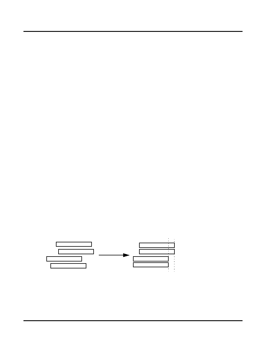
Figure 11. Dual Channel Alignment
Channel AD
Channel BC
Channel BD
Channel AC
Channel AD
Channel BC
Channel BD
Channel AC
t1 t0
DUAL ALIGNMENT OF CHANNELS AC AND AD
DUAL ALIGNMENT OF CHANNELS BC AND BD
相關(guān)PDF資料 |
PDF描述 |
|---|---|
| PIC32MX775F512H-80I/MR | IC MCU 32BIT 512KB FLASH 64QFN |
| VI-J4H-IW-F1 | CONVERTER MOD DC/DC 52V 100W |
| PIC18F4682-I/PT | IC PIC MCU FLASH 40KX16 44TQFP |
| ORSO82G5-1FN680I | IC TRANCEIVERS FPSC 680FPBGA |
| PIC32MX775F256L-80I/PT | IC MCU 32BIT 256K FLASH 100TQFP |
相關(guān)代理商/技術(shù)參數(shù) |
參數(shù)描述 |
|---|---|
| ORT82G5-3FN680C1 | 功能描述:FPGA - 現(xiàn)場可編程門陣列 10368 LUT 372 I/O RoHS:否 制造商:Altera Corporation 系列:Cyclone V E 柵極數(shù)量: 邏輯塊數(shù)量:943 內(nèi)嵌式塊RAM - EBR:1956 kbit 輸入/輸出端數(shù)量:128 最大工作頻率:800 MHz 工作電源電壓:1.1 V 最大工作溫度:+ 70 C 安裝風格:SMD/SMT 封裝 / 箱體:FBGA-256 |
| ORT82G5-FPSC-EV | 功能描述:可編程邏輯 IC 開發(fā)工具 Ev Eval Brd RoHS:否 制造商:Altera Corporation 產(chǎn)品:Development Kits 類型:FPGA 工具用于評估:5CEFA7F3 接口類型: 工作電源電壓: |
| ORT82G5-G2-PAC-EV | 功能描述:可編程邏輯 IC 開發(fā)工具 ORT82G5 ispGDX256 is pPAC PwrMgr 1208 BC RoHS:否 制造商:Altera Corporation 產(chǎn)品:Development Kits 類型:FPGA 工具用于評估:5CEFA7F3 接口類型: 工作電源電壓: |
| ORT8850 | 制造商:LATTICE 制造商全稱:Lattice Semiconductor 功能描述:Field-Programmable System Chip (FPSC) Eight-Channel x 850 Mbits/s Backplane Transceiver |
| ORT8850-FPSC-EV | 功能描述:可編程邏輯 IC 開發(fā)工具 ORCA ORT8850 FPSC Eval Brd RoHS:否 制造商:Altera Corporation 產(chǎn)品:Development Kits 類型:FPGA 工具用于評估:5CEFA7F3 接口類型: 工作電源電壓: |
發(fā)布緊急采購,3分鐘左右您將得到回復(fù)。