- 您現(xiàn)在的位置:買賣IC網(wǎng) > PDF目錄11733 > ORT82G5-3FN680C (Lattice Semiconductor Corporation)IC TRANCEIVERS FPSC 680FPBGA PDF資料下載
參數(shù)資料
| 型號(hào): | ORT82G5-3FN680C |
| 廠商: | Lattice Semiconductor Corporation |
| 文件頁數(shù): | 97/119頁 |
| 文件大小: | 0K |
| 描述: | IC TRANCEIVERS FPSC 680FPBGA |
| 產(chǎn)品變化通告: | Product Discontinuation 01/Aug/2011 |
| 標(biāo)準(zhǔn)包裝: | 24 |
| 系列: | * |
第1頁第2頁第3頁第4頁第5頁第6頁第7頁第8頁第9頁第10頁第11頁第12頁第13頁第14頁第15頁第16頁第17頁第18頁第19頁第20頁第21頁第22頁第23頁第24頁第25頁第26頁第27頁第28頁第29頁第30頁第31頁第32頁第33頁第34頁第35頁第36頁第37頁第38頁第39頁第40頁第41頁第42頁第43頁第44頁第45頁第46頁第47頁第48頁第49頁第50頁第51頁第52頁第53頁第54頁第55頁第56頁第57頁第58頁第59頁第60頁第61頁第62頁第63頁第64頁第65頁第66頁第67頁第68頁第69頁第70頁第71頁第72頁第73頁第74頁第75頁第76頁第77頁第78頁第79頁第80頁第81頁第82頁第83頁第84頁第85頁第86頁第87頁第88頁第89頁第90頁第91頁第92頁第93頁第94頁第95頁第96頁當(dāng)前第97頁第98頁第99頁第100頁第101頁第102頁第103頁第104頁第105頁第106頁第107頁第108頁第109頁第110頁第111頁第112頁第113頁第114頁第115頁第116頁第117頁第118頁第119頁
Lattice Semiconductor
ORCA ORT42G5 and ORT82G5 Data Sheet
79
External Reference Clock
The external reference clock selection and its interface are a critical part of system applications for this product.
Table 38 species reference clock requirements, over the full range of operating conditions. The designer is
encourage to read TN1040, SERDES Reference Clock, which discusses various aspects of this system element
and its interconnection.
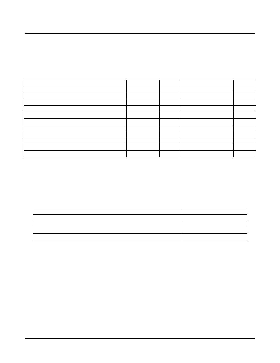
Table 38. Reference Clock Specications (REFCLKP and REFCLKN)
Embedded Core Timing Characteristics
Table 39 summarizes the end-to-end latencies through the embedded core for the various modes. All latencies are
given in clock cycles for system clocks at half the REFCLK_[A:B] frequency. For a REFCLK_[A:B] of 156.25 MHz, a
system clock cycle is 6.4 ns.
Table 39. Signal Latencies, Embedded Core
Parameter
Min.
Typ.
Max.
Units
Frequency Range
60
—
185
MHz
Frequency Tolerance
1
-350
—
350
ppm
Duty Cycle (Measured at 50% Amplitude Point)
40
50
60
%
Rise Time
—
500
1000
ps
Fall Time
—
500
1000
ps
P–N Input Skew
—
75
ps
Differential Amplitude
500
800
2 x VDDIB
mVp-p
Common Mode Level
Vsingle-ended/2
0.75
VDD15 – (Vsingle-ended/2)
V
Single-Ended Amplitude
250
400
VDDIB
mVp-p
Input Capacitance (at REFCLKP)
—
5
pF
Input Capacitance (at REFCLKN)
—
5
pF
1. This specication indicates the capability of the high speed receiver CDR PLL to acquire lock when the reference clock frequency and
incoming data rate are not synchronized.
Operating Mode
Signal Latency (max.)
Transmit Path
5 clock cycles
Receive Path
Multi-Channel Alignment Bypassed
1
4.5 clock cycles
With Multi-Channel Alignment
1
13.5-22.5 clock cycles
1. With multi-channel alignment, the latency is largest when the skew between channels is at the maximum that can be correctly
compensated for (18 clock cycles). The latency specied in the table is for data from the channel received rst.
相關(guān)PDF資料 |
PDF描述 |
|---|---|
| PIC32MX775F512H-80I/MR | IC MCU 32BIT 512KB FLASH 64QFN |
| VI-J4H-IW-F1 | CONVERTER MOD DC/DC 52V 100W |
| PIC18F4682-I/PT | IC PIC MCU FLASH 40KX16 44TQFP |
| ORSO82G5-1FN680I | IC TRANCEIVERS FPSC 680FPBGA |
| PIC32MX775F256L-80I/PT | IC MCU 32BIT 256K FLASH 100TQFP |
相關(guān)代理商/技術(shù)參數(shù) |
參數(shù)描述 |
|---|---|
| ORT82G5-3FN680C1 | 功能描述:FPGA - 現(xiàn)場(chǎng)可編程門陣列 10368 LUT 372 I/O RoHS:否 制造商:Altera Corporation 系列:Cyclone V E 柵極數(shù)量: 邏輯塊數(shù)量:943 內(nèi)嵌式塊RAM - EBR:1956 kbit 輸入/輸出端數(shù)量:128 最大工作頻率:800 MHz 工作電源電壓:1.1 V 最大工作溫度:+ 70 C 安裝風(fēng)格:SMD/SMT 封裝 / 箱體:FBGA-256 |
| ORT82G5-FPSC-EV | 功能描述:可編程邏輯 IC 開發(fā)工具 Ev Eval Brd RoHS:否 制造商:Altera Corporation 產(chǎn)品:Development Kits 類型:FPGA 工具用于評(píng)估:5CEFA7F3 接口類型: 工作電源電壓: |
| ORT82G5-G2-PAC-EV | 功能描述:可編程邏輯 IC 開發(fā)工具 ORT82G5 ispGDX256 is pPAC PwrMgr 1208 BC RoHS:否 制造商:Altera Corporation 產(chǎn)品:Development Kits 類型:FPGA 工具用于評(píng)估:5CEFA7F3 接口類型: 工作電源電壓: |
| ORT8850 | 制造商:LATTICE 制造商全稱:Lattice Semiconductor 功能描述:Field-Programmable System Chip (FPSC) Eight-Channel x 850 Mbits/s Backplane Transceiver |
| ORT8850-FPSC-EV | 功能描述:可編程邏輯 IC 開發(fā)工具 ORCA ORT8850 FPSC Eval Brd RoHS:否 制造商:Altera Corporation 產(chǎn)品:Development Kits 類型:FPGA 工具用于評(píng)估:5CEFA7F3 接口類型: 工作電源電壓: |
發(fā)布緊急采購,3分鐘左右您將得到回復(fù)。