- 您現(xiàn)在的位置:買賣IC網(wǎng) > PDF目錄11733 > ORT82G5-3FN680C (Lattice Semiconductor Corporation)IC TRANCEIVERS FPSC 680FPBGA PDF資料下載
參數(shù)資料
| 型號(hào): | ORT82G5-3FN680C |
| 廠商: | Lattice Semiconductor Corporation |
| 文件頁數(shù): | 70/119頁 |
| 文件大?。?/td> | 0K |
| 描述: | IC TRANCEIVERS FPSC 680FPBGA |
| 產(chǎn)品變化通告: | Product Discontinuation 01/Aug/2011 |
| 標(biāo)準(zhǔn)包裝: | 24 |
| 系列: | * |
第1頁第2頁第3頁第4頁第5頁第6頁第7頁第8頁第9頁第10頁第11頁第12頁第13頁第14頁第15頁第16頁第17頁第18頁第19頁第20頁第21頁第22頁第23頁第24頁第25頁第26頁第27頁第28頁第29頁第30頁第31頁第32頁第33頁第34頁第35頁第36頁第37頁第38頁第39頁第40頁第41頁第42頁第43頁第44頁第45頁第46頁第47頁第48頁第49頁第50頁第51頁第52頁第53頁第54頁第55頁第56頁第57頁第58頁第59頁第60頁第61頁第62頁第63頁第64頁第65頁第66頁第67頁第68頁第69頁當(dāng)前第70頁第71頁第72頁第73頁第74頁第75頁第76頁第77頁第78頁第79頁第80頁第81頁第82頁第83頁第84頁第85頁第86頁第87頁第88頁第89頁第90頁第91頁第92頁第93頁第94頁第95頁第96頁第97頁第98頁第99頁第100頁第101頁第102頁第103頁第104頁第105頁第106頁第107頁第108頁第109頁第110頁第111頁第112頁第113頁第114頁第115頁第116頁第117頁第118頁第119頁
Lattice Semiconductor
ORCA ORT42G5 and ORT82G5 Data Sheet
54
Parallel Loopback at the SERDES Boundary
In this parallel loopback differential data are received at the HDINP_xx and HDINN_xx pins and are retransmitted
at the HDOUTP_xx and HDOUTN_xx pins. The loopback path is at the interface between the SERDES blocks and
the MUX and DEMUX blocks and uses the parallel 10-bit buses at these interfaces (see Figure 32b). The loopback
connection is made such that the input signals to the TX SERDES block is the same as the output signals from the
RX SERDES block. In this parallel loopback mode, the MRWDxx[39:0] signal lines remain active and the
TWDxx[31:0], TCOMMAxx[3:0] and TBIT9xx[3:0] signal lines are not used. This mode is normally used for tests
where serial test data is received from and transmitted to either test equipment or via a serial backplane to a
remote card and is the basic loopback path shown earlier in Figure 32(b).
The data rate selection bits TXHR and RXHR in the channel conguration registers must be congured to carry the
same value. Also, the 8b/10b encoder and decoder are excluded from the loopback path by setting the 8b10bT and
8b10bR conguration bits to 0. Table 21 and Table 22 illustrate the control interface register conguration for the
parallel loopback.
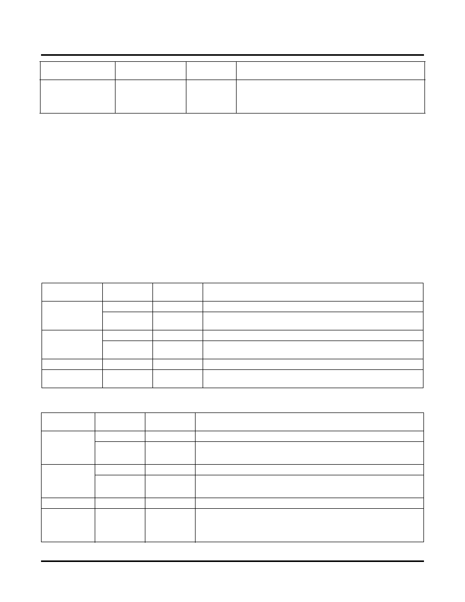
Table 21. Parallel Loopback at the SERDES Boundary Conguration Bit Denitions
Table 22. Parallel Loopback at the SERDES Boundary Conguration Bit Denitions for the ORT82G5
30801, 30901
Bit 0 =1 (Channel A)
Bit 1 = 1 (Channel B)
Bit 2 = 1 (Channel C)
Bit 3 = 1 (Channel D)
LOOPENB_xx Set any of the bits 0-3 to 1 to do serial loopback on the corre-
sponding channel.* The high speed serial outputs will not be
active.
*This test mode can also be set using TESTEN_xx in place of LOOPENB_xx. In that case, Test Mode must be set to 00000.
Register
Address (Hex)
Bit Value
Bit Name
Comments
30022, 30032,
30122, 30132
Bit 0 = 0 or 1
TXHR
Set to 0 or 1. TXHR and RXHR bits must be set to the same value.
Bit 7 = 0
8b10bT
Set to 0 The 8b/10b encoder is excluded from the loopback path. The
8b/10b encoder and decoder selection control bits must both be set to 0.
30023, 30033,
30123, 30133
Bit 0 = 0 or 1
RXHR
Set to 0 or 1. TXHR and RXHR bits must be set to the same value.
Bit 3 = 0
8b10bR
Set to 0.The 8b/10b decoder is excluded from the loopback path. The
8b/10b encoder and decoder selection control bits must both be set to 0.
30005, 30105
Bit 7 = 1
GTESTEN
SET to 1 if the loopback is done globally on both channels.
30026, 30036,
30126, 30136
Bits[4:0]
Testmode
Set to 00001
Register
Address (Hex)
Bit Value
Bit Name
Comments
30002, 30012,
30022, 30032,
30102, 30112,
30122, 30132
Bit 0 = 0 or 1
TXHR
Set to 0 or 1. TXHR and RXHR bits must be set to the same value.
Bit 7 = 0
8b10bT
Set to 0 The 8b/10b encoder is excluded from the loopback path. The
8b/10b encoder and decoder selection control bits must both be set to 0.
30003, 30013,
30023, 30033,
30103, 30113,
30123, 30133
Bit 0 = 0 or 1
RXHR
Set to 0 or 1. TXHR and RXHR bits must be set to the same value.
Bit 3 = 0
8b10bR
Set to 0.The 8b/10b decoder is excluded from the loopback path. The
8b/10b encoder and decoder selection control bits must both be set to 0.
30005, 30105
Bit 7 = 1
GTESTEN
SET to 1 if the loopback is done globally on all four channels.
30006, 30016,
30026, 30036,
30106, 30116,
30126, 30136
Bits[4:0]
Testmode
Set to 00001
Register
Address
Bit Value
Bit Name
Comments
相關(guān)PDF資料 |
PDF描述 |
|---|---|
| PIC32MX775F512H-80I/MR | IC MCU 32BIT 512KB FLASH 64QFN |
| VI-J4H-IW-F1 | CONVERTER MOD DC/DC 52V 100W |
| PIC18F4682-I/PT | IC PIC MCU FLASH 40KX16 44TQFP |
| ORSO82G5-1FN680I | IC TRANCEIVERS FPSC 680FPBGA |
| PIC32MX775F256L-80I/PT | IC MCU 32BIT 256K FLASH 100TQFP |
相關(guān)代理商/技術(shù)參數(shù) |
參數(shù)描述 |
|---|---|
| ORT82G5-3FN680C1 | 功能描述:FPGA - 現(xiàn)場(chǎng)可編程門陣列 10368 LUT 372 I/O RoHS:否 制造商:Altera Corporation 系列:Cyclone V E 柵極數(shù)量: 邏輯塊數(shù)量:943 內(nèi)嵌式塊RAM - EBR:1956 kbit 輸入/輸出端數(shù)量:128 最大工作頻率:800 MHz 工作電源電壓:1.1 V 最大工作溫度:+ 70 C 安裝風(fēng)格:SMD/SMT 封裝 / 箱體:FBGA-256 |
| ORT82G5-FPSC-EV | 功能描述:可編程邏輯 IC 開發(fā)工具 Ev Eval Brd RoHS:否 制造商:Altera Corporation 產(chǎn)品:Development Kits 類型:FPGA 工具用于評(píng)估:5CEFA7F3 接口類型: 工作電源電壓: |
| ORT82G5-G2-PAC-EV | 功能描述:可編程邏輯 IC 開發(fā)工具 ORT82G5 ispGDX256 is pPAC PwrMgr 1208 BC RoHS:否 制造商:Altera Corporation 產(chǎn)品:Development Kits 類型:FPGA 工具用于評(píng)估:5CEFA7F3 接口類型: 工作電源電壓: |
| ORT8850 | 制造商:LATTICE 制造商全稱:Lattice Semiconductor 功能描述:Field-Programmable System Chip (FPSC) Eight-Channel x 850 Mbits/s Backplane Transceiver |
| ORT8850-FPSC-EV | 功能描述:可編程邏輯 IC 開發(fā)工具 ORCA ORT8850 FPSC Eval Brd RoHS:否 制造商:Altera Corporation 產(chǎn)品:Development Kits 類型:FPGA 工具用于評(píng)估:5CEFA7F3 接口類型: 工作電源電壓: |
發(fā)布緊急采購(gòu),3分鐘左右您將得到回復(fù)。