- 您現在的位置:買賣IC網 > PDF目錄373274 > RIVA128 (意法半導體) RIVA 128⑩ 128-BIT 3D MULTIMEDIA ACCELERATOR PDF資料下載
參數資料
| 型號: | RIVA128 |
| 廠商: | 意法半導體 |
| 英文描述: | RIVA 128⑩ 128-BIT 3D MULTIMEDIA ACCELERATOR |
| 中文描述: | 麗娃128⑩128位3D多媒體加速器 |
| 文件頁數: | 51/85頁 |
| 文件大小: | 609K |
| 代理商: | RIVA128 |
第1頁第2頁第3頁第4頁第5頁第6頁第7頁第8頁第9頁第10頁第11頁第12頁第13頁第14頁第15頁第16頁第17頁第18頁第19頁第20頁第21頁第22頁第23頁第24頁第25頁第26頁第27頁第28頁第29頁第30頁第31頁第32頁第33頁第34頁第35頁第36頁第37頁第38頁第39頁第40頁第41頁第42頁第43頁第44頁第45頁第46頁第47頁第48頁第49頁第50頁當前第51頁第52頁第53頁第54頁第55頁第56頁第57頁第58頁第59頁第60頁第61頁第62頁第63頁第64頁第65頁第66頁第67頁第68頁第69頁第70頁第71頁第72頁第73頁第74頁第75頁第76頁第77頁第78頁第79頁第80頁第81頁第82頁第83頁第84頁第85頁
128-BIT 3D MULTIMEDIA ACCELERATOR
RIVA128ZX
51/85
8.4
Table 15 shows the Video Port pin definition when
the RIVA128ZX is configured inITU-R-656 Master
Mode. Before enteringthis mode,RIVA128ZX dis-
ables all Video Port devices so that the bus is tri-
stated. The RIVA128ZX will then enable the video
656 master device through the serial bus. In this
mode, the video device outputs the video data
continuously at the PIXCLK rate.
656 MASTER MODE
Table 15.
656 master mode pin definition
The 656 Master Mode assumes that
VID[7:0]
and
PIXCLK
can be tri-stated when the slave is inac-
tive. If a slave cannot tri-state all its signals, an ex-
ternal tri-state buffer is needed.
Video data capture
Video Port pixeldata is clocked into the port by the
external pixel clock and then passed to the
RIVA128ZX’s video capture FIFO.
Pixel data capture is controlled by the ITU-R-656
codes embedded in the data stream; each active
line beginning with SAV (start active video) and
ending with EAV (end active video).
In normal operation, when SAV = x00, capture of
video data begins, and when EAV = xx1, capture
of video data ends for that line. When VBI (Vertical
Blanking Interval)capture is active, theserules are
modified.
656 master mode timing specification
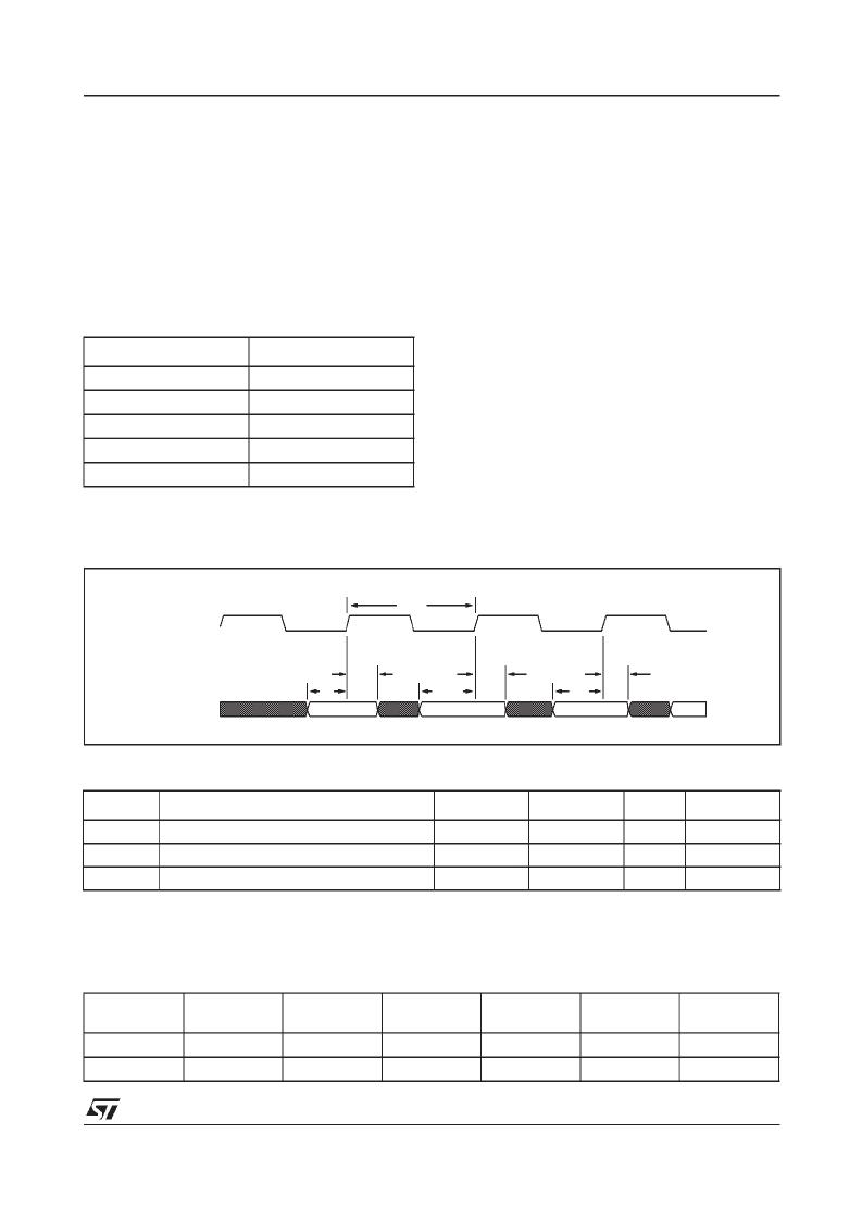
Figure 62.
656 Master Mode timing diagram
Table 16.
ITU-R-656 Master Mode timing parameters
NOTE
1
VACTIVE
indicates that valid pixel data is being transmitted across the video port.
Table 17.
YUV (YCbCr) byte ordering
Normal Mode
656 Master Mode
MPCLK
PIXCLK
MPAD[7:0]
VID[7:0]
MPFRAME#
Not used
MPDTACK#
Not used
MPSTOP#
Not used
Symbol
Parameter
Min.
Max.
Unit
Notes
t
3
t
4
t
5
VID[7:0]
hold from
PIXCLK
high
0
ns
VID[7:0]
setup to
PIXCLK
high
5
ns
PIXCLK
cycle time
35
ns
1st byte
2nd byte
3rd byte
4th byte
5th (next
dword)
6th byte
7th byte
U[7:0]
Y0[7:0]
V[7:0]
Y1[7:0]
U[7:0]
Y0[7:0]
V[7:0]
Cb[7:0]
Y0[7:0]
Cr[7:0]
Y1[7:0]
Cb[7:0]
Y0[7:0]
Cr[7:0]
t
5
t
4
t
3
t
4
t
3
t
4
t
3
PIXCLK
VID[7:0]
相關PDF資料 |
PDF描述 |
|---|---|
| RIX-0142-H | FILTER IEC EINGANG ULTRA KOMPAKT 1A |
| RIX-0342-H | FILTER IEC EINGANG ULTRA KOMPAKT 3A |
| RIX-0642-H | FILTER IEC EINGANG ULTRA KOMPAKT 6A |
| RJ45SRB-BLACK | TUELLE FUER RJ45 STECKER SW Inhalt pro Packung: 8 Stk. |
| RJ45SRB-BLUE | TUELLE FUER RJ45 STECKER BLAU Inhalt pro Packung: 8 Stk. |
相關代理商/技術參數 |
參數描述 |
|---|---|
| RIVA128ZX | 制造商:STMicroelectronics 功能描述:128-BIT 3D MULTIMEDIA ACCELERATOR, PBGA300 |
| RIVCF256H | 制造商:STEC Inc 功能描述:256MB COMPACT FLASH - Bulk |
| RIVET DPG FLOAT MTG | 制造商:ITT Interconnect Solutions 功能描述:Rack & Panel |
| RIVET(SSR389) | 制造商: 功能描述: 制造商:undefined 功能描述: |
| RIVET-DPD-PIN-INSERT-SPCR | 制造商:ITT Interconnect Solutions 功能描述: |
發(fā)布緊急采購,3分鐘左右您將得到回復。