- 您現(xiàn)在的位置:買賣IC網(wǎng) > PDF目錄373274 > RIVA128 (意法半導體) RIVA 128⑩ 128-BIT 3D MULTIMEDIA ACCELERATOR PDF資料下載
參數(shù)資料
| 型號: | RIVA128 |
| 廠商: | 意法半導體 |
| 英文描述: | RIVA 128⑩ 128-BIT 3D MULTIMEDIA ACCELERATOR |
| 中文描述: | 麗娃128⑩128位3D多媒體加速器 |
| 文件頁數(shù): | 64/85頁 |
| 文件大?。?/td> | 609K |
| 代理商: | RIVA128 |
第1頁第2頁第3頁第4頁第5頁第6頁第7頁第8頁第9頁第10頁第11頁第12頁第13頁第14頁第15頁第16頁第17頁第18頁第19頁第20頁第21頁第22頁第23頁第24頁第25頁第26頁第27頁第28頁第29頁第30頁第31頁第32頁第33頁第34頁第35頁第36頁第37頁第38頁第39頁第40頁第41頁第42頁第43頁第44頁第45頁第46頁第47頁第48頁第49頁第50頁第51頁第52頁第53頁第54頁第55頁第56頁第57頁第58頁第59頁第60頁第61頁第62頁第63頁當前第64頁第65頁第66頁第67頁第68頁第69頁第70頁第71頁第72頁第73頁第74頁第75頁第76頁第77頁第78頁第79頁第80頁第81頁第82頁第83頁第84頁第85頁
128-BIT 3D MULTIMEDIA ACCELERATOR
RIVA128ZX
64/85
13
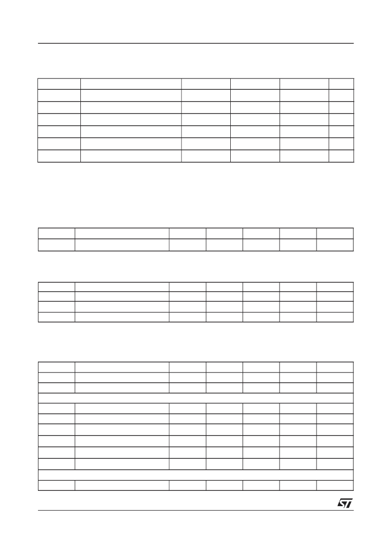
13.1 ABSOLUTE MAXIMUM RATINGS
1
ELECTRICAL SPECIFICATIONS
NOTES
1
Stresses greater than those listed under ‘Absolute maximum ratings’ may cause permanent damage to the device. This
is a stress rating only andfunctional operation of the device at these or any other conditions above those indicated in the
operational sections of this specification is not implied.Exposure to absolute maximum rating conditions for extended pe-
riods may affect reliability.
For 3V tolerant pins VDD = 3.3V
±
0.3V, for 5V tolerant pins (PCI, Video Port and Serial interfaces) VDD = 5V
±
0.5V
2
13.2 OPERATING CONDITIONS
13.3 DC SPECIFICATIONS
Table 22.
DC characteristics
NOTES
1
2
Includes high impedance output leakage for all bi-directional buffers with tri-state outputs
VDD = max, GND
≤
VIN
≤
VDD
Table 23.
Parameters applying to PCI and AGP interface pins
Symbol
Parameter
Min.
Max.
Units
Notes
VDD/AVDD
DC supply voltage
3.6
V
Voltage on input and output pins
GND-1.0
VDD+0.5
V
2
TS
Storage temperature (ambient)
-55
125
°
C
TA
Temperature under bias
0
85
°
C
Analog output current (per output)
45
mA
DC digital output current (per output)
25
mA
Symbol
Parameter
Min.
Typ.
Max.
Units
Notes
TC
Case temperature
120
°
C
Symbol
VDD
IIN
Parameter
Positive supply voltage
Input current (signal pins)
Min.
3.135
Typ.
3.3
Max.
3.465
±
10
Units
V
μ
A
Notes
1, 2
Power dissipation
3.7
W
Symbol
CIN
Parameter
Input capacitance
Min.
5
Typ.
Max.
10
Units
pF
Notes
1
COUT
Output load capacitance
5
50
pF
1
Parameters for 5V signaling environment only:
VIH
Input logic 1 voltage
2.0
5.75
V
VIL
Input logic 0 voltage
-0.5
0.8
V
VOH
Output logic 1 level
2.4
V
VOL
Output logic 0 level
0.55
V
IOH
Output load current, logic 1 level
-2
mA
IOL
Output load current, logic 0 level
3 or 6
mA
2
Parameters for 3.3V and AGP signaling environments only:
VIH
Input logic 1 voltage
0.475VDD
VDD+0.5
V
相關PDF資料 |
PDF描述 |
|---|---|
| RIX-0142-H | FILTER IEC EINGANG ULTRA KOMPAKT 1A |
| RIX-0342-H | FILTER IEC EINGANG ULTRA KOMPAKT 3A |
| RIX-0642-H | FILTER IEC EINGANG ULTRA KOMPAKT 6A |
| RJ45SRB-BLACK | TUELLE FUER RJ45 STECKER SW Inhalt pro Packung: 8 Stk. |
| RJ45SRB-BLUE | TUELLE FUER RJ45 STECKER BLAU Inhalt pro Packung: 8 Stk. |
相關代理商/技術參數(shù) |
參數(shù)描述 |
|---|---|
| RIVA128ZX | 制造商:STMicroelectronics 功能描述:128-BIT 3D MULTIMEDIA ACCELERATOR, PBGA300 |
| RIVCF256H | 制造商:STEC Inc 功能描述:256MB COMPACT FLASH - Bulk |
| RIVET DPG FLOAT MTG | 制造商:ITT Interconnect Solutions 功能描述:Rack & Panel |
| RIVET(SSR389) | 制造商: 功能描述: 制造商:undefined 功能描述: |
| RIVET-DPD-PIN-INSERT-SPCR | 制造商:ITT Interconnect Solutions 功能描述: |
發(fā)布緊急采購,3分鐘左右您將得到回復。