- 您現(xiàn)在的位置:買賣IC網(wǎng) > PDF目錄383876 > T7633 (Lineage Power) Dual T1/E1 3.3 V Short-Haul Terminator(雙T1/E1 3.3V短通信距離終端器) PDF資料下載
參數(shù)資料
| 型號: | T7633 |
| 廠商: | Lineage Power |
| 英文描述: | Dual T1/E1 3.3 V Short-Haul Terminator(雙T1/E1 3.3V短通信距離終端器) |
| 中文描述: | 雙T1/E1的3.3伏短途終結(jié)者(雙T1/E1的3.3短通信距離終端器) |
| 文件頁數(shù): | 32/248頁 |
| 文件大小: | 1459K |
| 代理商: | T7633 |
第1頁第2頁第3頁第4頁第5頁第6頁第7頁第8頁第9頁第10頁第11頁第12頁第13頁第14頁第15頁第16頁第17頁第18頁第19頁第20頁第21頁第22頁第23頁第24頁第25頁第26頁第27頁第28頁第29頁第30頁第31頁當(dāng)前第32頁第33頁第34頁第35頁第36頁第37頁第38頁第39頁第40頁第41頁第42頁第43頁第44頁第45頁第46頁第47頁第48頁第49頁第50頁第51頁第52頁第53頁第54頁第55頁第56頁第57頁第58頁第59頁第60頁第61頁第62頁第63頁第64頁第65頁第66頁第67頁第68頁第69頁第70頁第71頁第72頁第73頁第74頁第75頁第76頁第77頁第78頁第79頁第80頁第81頁第82頁第83頁第84頁第85頁第86頁第87頁第88頁第89頁第90頁第91頁第92頁第93頁第94頁第95頁第96頁第97頁第98頁第99頁第100頁第101頁第102頁第103頁第104頁第105頁第106頁第107頁第108頁第109頁第110頁第111頁第112頁第113頁第114頁第115頁第116頁第117頁第118頁第119頁第120頁第121頁第122頁第123頁第124頁第125頁第126頁第127頁第128頁第129頁第130頁第131頁第132頁第133頁第134頁第135頁第136頁第137頁第138頁第139頁第140頁第141頁第142頁第143頁第144頁第145頁第146頁第147頁第148頁第149頁第150頁第151頁第152頁第153頁第154頁第155頁第156頁第157頁第158頁第159頁第160頁第161頁第162頁第163頁第164頁第165頁第166頁第167頁第168頁第169頁第170頁第171頁第172頁第173頁第174頁第175頁第176頁第177頁第178頁第179頁第180頁第181頁第182頁第183頁第184頁第185頁第186頁第187頁第188頁第189頁第190頁第191頁第192頁第193頁第194頁第195頁第196頁第197頁第198頁第199頁第200頁第201頁第202頁第203頁第204頁第205頁第206頁第207頁第208頁第209頁第210頁第211頁第212頁第213頁第214頁第215頁第216頁第217頁第218頁第219頁第220頁第221頁第222頁第223頁第224頁第225頁第226頁第227頁第228頁第229頁第230頁第231頁第232頁第233頁第234頁第235頁第236頁第237頁第238頁第239頁第240頁第241頁第242頁第243頁第244頁第245頁第246頁第247頁第248頁
Advance Data Sheet
T7633 Dual T1/E1 3.3 V Short-Haul Terminator
May 1998
22
Lucent Technologies Inc.
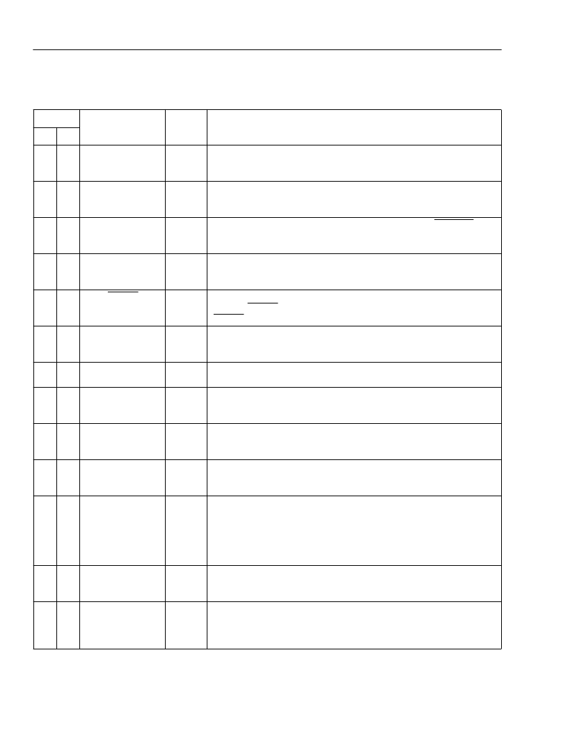
Pin Information
(continued)
Table 1. Pin Descriptions
(continued)
* I
U
indicates an internal pull-up.
Pin
Symbol
Type
*
Description
C1
C2
137
45
TND
O
Transmit Line Interface Negative-Rail Data.
This signal is the
transmit framer negative NRZ output data. Data changes on the rising
edge of TLCK. In the single-rail mode, TND = 0.
Transmit Framer Line Interface Clock.
Optional 1.544 MHz DS1 or
2.048 MHz output signal from the transmit framer. TND and TPD data
changes on the rising edge of TLCK.
Receive Framer Line Interface Clock.
Valid when the FRAMER pin is
strapped to 0 V. This is the 1.544 MHz DS1 or 2.048 MHz input clock
signal used by the receive framer to latch RPD and RND data.
Receive Framer Clock.
Output receive framer clock signal used to
clock out the receive framer output signals. In normal operation, this is
the recovered receive line clock signal.
LIU System Clock Mode.
This pin selects either a 16x rate clock for
SYSCK (CKSEL = 1) or a primary line rate clock for SYSCK
(CKSEL = 0).
Receive Framer Data.
This signal is the decoded data input to the
receive elastic store. During loss of frame alignment, this signal is
forced to 1.
Receive Frame Sync.
This active-high signal is the 8 kHz frame
synchronization pulse generated by the receive framer.
Receive Framer Signaling Superframe Sync.
This active-high signal
is the CEPT signaling superframe (multiframe) synchronization pulse
in the receive framer.
Receive Framer CRC-4 Multiframe Sync.
This active-high signal is
the CEPT CRC-4 multiframe synchronization pulse in the receive
framer.
Receive Facility Data Link Clock.
In DS1-DDS with data link access,
this is an 8 kHz clock signal. Otherwise, this is a 4 kHz clock signal.
The receive data link bit changes on the falling edge of RFDLCK.
Receive Facility Data Link.
Serial output facility data link bit stream
extracted from the receive line data stream by the receive framer. In
DS1-DDS with data link access, this is an 8 kbits/s signal; otherwise,
4 kbits/s. In the CEPT frame format, RFDL can be programmed to one
of the Sa bits of the NOT FAS frame TS0. During loss of frame
alignment, this signal is 1.
Transmit Concentration Highway Interface (CHI) Clock.
2.048 MHz, 4.096 MHz, 8.192 MHz, or 16.384 MHz. This clock must
be free of jitter.
Transmit CHI Frame Sync.
Transmit CHI
8 kHz input frame
synchronization pulse phase-locked to TCHICK. In the CHI master
mode, the transmit CHI generates the 8 kHz frame sync to control the
CHI.
136
46
TLCK
O
135
47
RLCK
I
134
49
RFRMCK
O
133
48
CKSEL
I
u
132
50
RFRMDATA
O
131
51
RFS
O
130
52
RSSFS
O
129
53
RCRCMFS
O
128
54
RFDLCK
O
127
55
RFDL
O
126
56
TCHICK
I
125
57
TCHIFS
I/O
相關(guān)PDF資料 |
PDF描述 |
|---|---|
| T7688 | 5.0 V E1/CEPT Quad Line Interface(5.0 V E1/CEPT四線接口) |
| T7689 | 5.0 V T1 Quad Line Interface(5.0 V T1四線接口) |
| T7690 | 5.0 V T1/E1 Quad Line Interface(5.0 V T1/E1 四線接口) |
| T7693 | 3.3 V T1/E1 Quad Line Interface( 3.3 V T1/E四線接口) |
| T7698 | Quad T1/E1 Line Interface and Octal T1/E1 Monitor(四T1/E1線接口和八T1/E1監(jiān)控器) |
相關(guān)代理商/技術(shù)參數(shù) |
參數(shù)描述 |
|---|---|
| T7645036 | 功能描述:手工工具 Campbell Snap Link #2450, 7/16", Steel RoHS:否 制造商:Molex 產(chǎn)品:Extraction Tools 類型: 描述/功能:Extraction tool |
| T7645106 | 制造商:COOPER INDUSTRIES 功能描述:CC ACCESYS / #7350 1/8 Quick Link Steel Zinc Plated UPC Tagged |
| T7645126 | 制造商:COOPER INDUSTRIES 功能描述:CC ACCESYS / #7350 1/4 Quick Link Steel Zinc Plated UPC Tagged |
| T7645136V | 制造商:COOPER INDUSTRIES 功能描述:CC ACCESYS / #7350 5/16 Quick Link Steel Zinc Plated UPC Tagged |
| T7645146 | 制造商:COOPER INDUSTRIES 功能描述:CC ACCESYS / #7350 3/8 Quick Link Steel Zinc Plated UPC Tagged |
發(fā)布緊急采購,3分鐘左右您將得到回復(fù)。