- 您現(xiàn)在的位置:買賣IC網(wǎng) > PDF目錄300038 > TMS320C2812ZHHS (TEXAS INSTRUMENTS INC) 16-BIT, 150 MHz, OTHER DSP, PBGA179 PDF資料下載
參數(shù)資料
| 型號(hào): | TMS320C2812ZHHS |
| 廠商: | TEXAS INSTRUMENTS INC |
| 元件分類: | 數(shù)字信號(hào)處理 |
| 英文描述: | 16-BIT, 150 MHz, OTHER DSP, PBGA179 |
| 封裝: | LEAD FREE, BGA-179 |
| 文件頁(yè)數(shù): | 72/156頁(yè) |
| 文件大小: | 1826K |
| 代理商: | TMS320C2812ZHHS |
第1頁(yè)第2頁(yè)第3頁(yè)第4頁(yè)第5頁(yè)第6頁(yè)第7頁(yè)第8頁(yè)第9頁(yè)第10頁(yè)第11頁(yè)第12頁(yè)第13頁(yè)第14頁(yè)第15頁(yè)第16頁(yè)第17頁(yè)第18頁(yè)第19頁(yè)第20頁(yè)第21頁(yè)第22頁(yè)第23頁(yè)第24頁(yè)第25頁(yè)第26頁(yè)第27頁(yè)第28頁(yè)第29頁(yè)第30頁(yè)第31頁(yè)第32頁(yè)第33頁(yè)第34頁(yè)第35頁(yè)第36頁(yè)第37頁(yè)第38頁(yè)第39頁(yè)第40頁(yè)第41頁(yè)第42頁(yè)第43頁(yè)第44頁(yè)第45頁(yè)第46頁(yè)第47頁(yè)第48頁(yè)第49頁(yè)第50頁(yè)第51頁(yè)第52頁(yè)第53頁(yè)第54頁(yè)第55頁(yè)第56頁(yè)第57頁(yè)第58頁(yè)第59頁(yè)第60頁(yè)第61頁(yè)第62頁(yè)第63頁(yè)第64頁(yè)第65頁(yè)第66頁(yè)第67頁(yè)第68頁(yè)第69頁(yè)第70頁(yè)第71頁(yè)當(dāng)前第72頁(yè)第73頁(yè)第74頁(yè)第75頁(yè)第76頁(yè)第77頁(yè)第78頁(yè)第79頁(yè)第80頁(yè)第81頁(yè)第82頁(yè)第83頁(yè)第84頁(yè)第85頁(yè)第86頁(yè)第87頁(yè)第88頁(yè)第89頁(yè)第90頁(yè)第91頁(yè)第92頁(yè)第93頁(yè)第94頁(yè)第95頁(yè)第96頁(yè)第97頁(yè)第98頁(yè)第99頁(yè)第100頁(yè)第101頁(yè)第102頁(yè)第103頁(yè)第104頁(yè)第105頁(yè)第106頁(yè)第107頁(yè)第108頁(yè)第109頁(yè)第110頁(yè)第111頁(yè)第112頁(yè)第113頁(yè)第114頁(yè)第115頁(yè)第116頁(yè)第117頁(yè)第118頁(yè)第119頁(yè)第120頁(yè)第121頁(yè)第122頁(yè)第123頁(yè)第124頁(yè)第125頁(yè)第126頁(yè)第127頁(yè)第128頁(yè)第129頁(yè)第130頁(yè)第131頁(yè)第132頁(yè)第133頁(yè)第134頁(yè)第135頁(yè)第136頁(yè)第137頁(yè)第138頁(yè)第139頁(yè)第140頁(yè)第141頁(yè)第142頁(yè)第143頁(yè)第144頁(yè)第145頁(yè)第146頁(yè)第147頁(yè)第148頁(yè)第149頁(yè)第150頁(yè)第151頁(yè)第152頁(yè)第153頁(yè)第154頁(yè)第155頁(yè)第156頁(yè)
Introduction
22
April 2001 Revised October 2005
SPRS174M
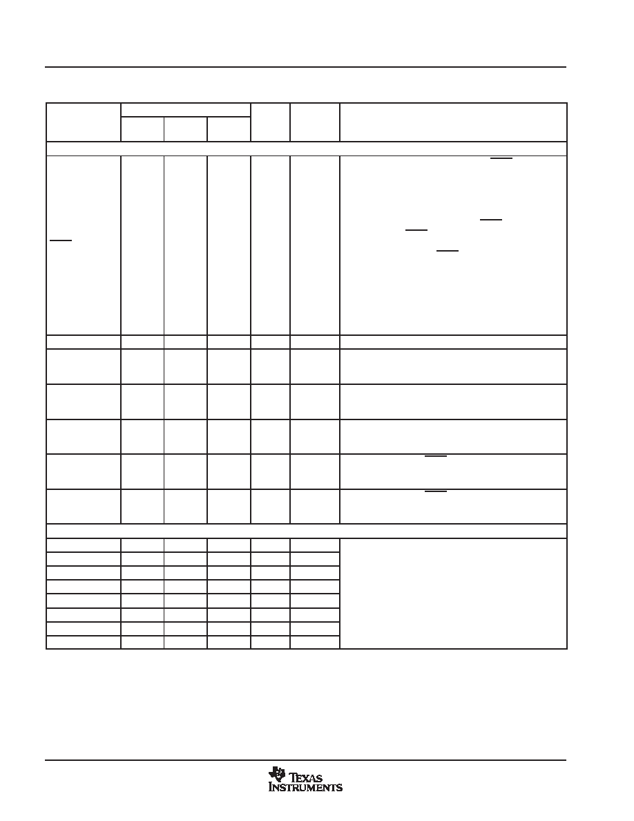
Table 22. Signal Descriptions (Continued)
NAME
DESCRIPTION
PU/PD§
I/O/Z
PIN NO.
NAME
DESCRIPTION
PU/PD§
I/O/Z
128-PIN
PBK
176-PIN
PGF
179-PIN
GHH
JTAG
TRST
B12
135
98
I
PD
JTAG test reset with internal pulldown. TRST, when driven
high, gives the scan system control of the operations of the
device. If this signal is not connected or driven low, the device
operates in its functional mode, and the test reset signals are
ignored.
NOTE: Do not use pullup resistors on TRST; it has an internal
pulldown device. TRST is an active high test pin and must be
maintained low at all times during normal device operation. In
a low-noise environment, TRST may be left floating. In other
instances,
an
external
pulldown
resistor
is
highly
recommended. The value of this resistor should be based on
drive strength of the debugger pods applicable to the design.
A 2.2-k
resistor generally offers adequate protection. Since
this is application-specific, it is recommended that each target
board be validated for proper operation of the debugger and
the application.
TCK
A12
136
99
I
PU
JTAG test clock with internal pullup
TMS
D13
126
92
I
PU
JTAG test-mode select (TMS) with internal pullup. This serial
control input is clocked into the TAP controller on the rising
edge of TCK.
TDI
C13
131
96
I
PU
JTAG test data input (TDI) with internal pullup. TDI is clocked
into the selected register (instruction or data) on a rising edge
of TCK.
TDO
D12
127
93
O/Z
JTAG scan out, test data output (TDO). The contents of the
selected register (instruction or data) is shifted out of TDO on
the falling edge of TCK.
EMU0
D11
137
100
I/O
PU
Emulator pin 0. When TRST is driven high, this pin is used
as an interrupt to or from the emulator system and is
defined as input/output through the JTAG scan.
EMU1
C9
146
105
I/O
PU
Emulator pin 1. When TRST is driven high, this pin is used
as an interrupt to or from the emulator system and is
defined as input/output through the JTAG scan.
ADC ANALOG INPUT SIGNALS
ADCINA7
B5
167
119
I
ADCINA6
D5
168
120
I
ADCINA5
E5
169
121
I
8-Channel analog inputs for Sample-and-Hold A. The ADC
ADCINA4
A4
170
122
I
8-Channel analog inputs for Sample-and-Hold A. The ADC
pins should not be driven before VDDA1, VDDA2, and VDDAIO
ADCINA3
B4
171
123
I
pins should not be driven before VDDA1, VDDA2, and VDDAIO
pins have been fully powered up.
ADCINA2
C4
172
124
I
pins have been fully powered up.
ADCINA1
D4
173
125
I
ADCINA0
A3
174
126
I
Typical drive strength of the output buffer for all pins is 4 mA except for TDO, XCLKOUT, XF, XINTF, EMU0, and EMU1 pins, which are 8 mA.
I = Input, O = Output, Z = High impedance
§ PU = pin has internal pullup; PD = pin has internal pulldown. Pullup/pulldown strength is given in Section 6.3.
相關(guān)PDF資料 |
PDF描述 |
|---|---|
| TMS320C6747BZKB4 | OTHER DSP, PBGA256 |
| TMS320LF2407APGEA | 16-BIT, 20 MHz, OTHER DSP, PQFP144 |
| TMS426409AP-60DJ | 4M X 4 EDO DRAM, 60 ns, PDSO24 |
| TMS426809AP-70DGC | 2M X 8 EDO DRAM, 70 ns, PDSO28 |
| TMS44400DJ-80 | 1M X 4 FAST PAGE DRAM, 80 ns, PDSO20 |
相關(guān)代理商/技術(shù)參數(shù) |
參數(shù)描述 |
|---|---|
| TMS320C28341 | 制造商:TI 制造商全稱:Texas Instruments 功能描述:Delfino Microcontrollers |
| TMS320C28341ZEPQ | 制造商:Texas Instruments 功能描述:DELFINO MICROCONTROLLER - Trays |
| TMS320C28341ZFEQ | 功能描述:32位微控制器 - MCU Delfino MCU RoHS:否 制造商:Texas Instruments 核心:C28x 處理器系列:TMS320F28x 數(shù)據(jù)總線寬度:32 bit 最大時(shí)鐘頻率:90 MHz 程序存儲(chǔ)器大小:64 KB 數(shù)據(jù) RAM 大小:26 KB 片上 ADC:Yes 工作電源電壓:2.97 V to 3.63 V 工作溫度范圍:- 40 C to + 105 C 封裝 / 箱體:LQFP-80 安裝風(fēng)格:SMD/SMT |
| TMS320C28341ZFET | 功能描述:32位微控制器 - MCU Delfino MCU RoHS:否 制造商:Texas Instruments 核心:C28x 處理器系列:TMS320F28x 數(shù)據(jù)總線寬度:32 bit 最大時(shí)鐘頻率:90 MHz 程序存儲(chǔ)器大小:64 KB 數(shù)據(jù) RAM 大小:26 KB 片上 ADC:Yes 工作電源電壓:2.97 V to 3.63 V 工作溫度范圍:- 40 C to + 105 C 封裝 / 箱體:LQFP-80 安裝風(fēng)格:SMD/SMT |
| TMS320C28341ZHHT | 功能描述:32位微控制器 - MCU Delfino MCU RoHS:否 制造商:Texas Instruments 核心:C28x 處理器系列:TMS320F28x 數(shù)據(jù)總線寬度:32 bit 最大時(shí)鐘頻率:90 MHz 程序存儲(chǔ)器大小:64 KB 數(shù)據(jù) RAM 大小:26 KB 片上 ADC:Yes 工作電源電壓:2.97 V to 3.63 V 工作溫度范圍:- 40 C to + 105 C 封裝 / 箱體:LQFP-80 安裝風(fēng)格:SMD/SMT |
發(fā)布緊急采購(gòu),3分鐘左右您將得到回復(fù)。