- 您現(xiàn)在的位置:買賣IC網(wǎng) > PDF目錄373714 > TS68230CP10 (意法半導(dǎo)體) HMOS PARALLEL INTERFACE/TIMER PDF資料下載
參數(shù)資料
| 型號(hào): | TS68230CP10 |
| 廠商: | 意法半導(dǎo)體 |
| 英文描述: | HMOS PARALLEL INTERFACE/TIMER |
| 中文描述: | HMO的并行接口/定時(shí)器 |
| 文件頁數(shù): | 25/61頁 |
| 文件大?。?/td> | 2911K |
| 代理商: | TS68230CP10 |
第1頁第2頁第3頁第4頁第5頁第6頁第7頁第8頁第9頁第10頁第11頁第12頁第13頁第14頁第15頁第16頁第17頁第18頁第19頁第20頁第21頁第22頁第23頁第24頁當(dāng)前第25頁第26頁第27頁第28頁第29頁第30頁第31頁第32頁第33頁第34頁第35頁第36頁第37頁第38頁第39頁第40頁第41頁第42頁第43頁第44頁第45頁第46頁第47頁第48頁第49頁第50頁第51頁第52頁第53頁第54頁第55頁第56頁第57頁第58頁第59頁第60頁第61頁
Programmable Options Mode 0 - Port A Submode 1X and Port B Submode 1X
(continued)
PBCR
0
X
H3 Status Control
H3 is an edge-sensitive status input, H3S is set by an asserted edge of H3.
3.4. MODE 1 - UNIDIRECTIONAL 16-BIT MODE
In mode 1, ports A and B are concatenated to form
a single 16-bit port. The port B submode field
controls the configuration of both ports. The possible
submodes are :
Port B Submode X0 - Pin-Definable Double-Buf-
fered Input or Single-Buffered Output
Port B Submode X1 - Pin-Definable Double-Buf-
fered Output or Non-Latched Input
Handshake pins H3 and H4, configured by program-
ming the port B control register, are associated with
the 16-bit double-buffered transfer. These 16-bit
transfers are enabled by setting the H34 enable bit
in the port general control register (PGCR). Hand-
shake pins H1 and H2 may be used as simple status
inputs not related to the 16-bit data transfer or H2
may be an output. Enabling of the H1 and H2 hands-
hake pins is done by setting the H12 enable bit of
the port general control register. The port A and B
data direction registers operate in each submode.
Along with the submode, they affect the data read
and written at the data register according to table
3.2. The data direction register also enables the out-
put buffer associated with each port pin. The DMA-
REQ pin may be associated only with H3.
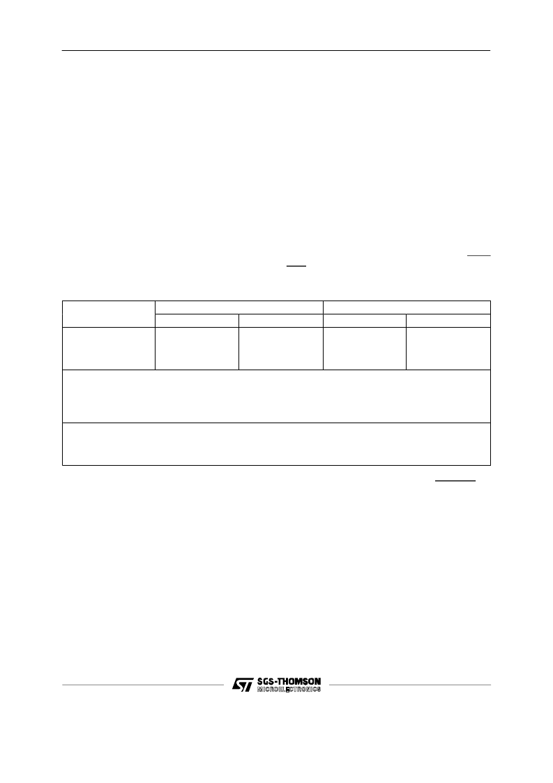
Table 3.2 :
Mode 1 Port Data Paths
.
Read Port A/B Register
DDR = 0
FIL, D. B.
Write Port A/B Register
DDR = 0
FOL, S. B.
Note 2
IOL/FOL, D. B.
Note 1
Mode
DDR = 1
FOL
Note 3
FOL
Note 3
DDR = 1
FOL, S. B.
Note 2
IOL/FOL, D. B.
Note 1
1, Port B
Submode X0
1, Port B
Submode X1
Note 1 : Data written to Port A goes to a temporary latch. When the Port B data register is later written, Port A
data is transferred to IOL/FOL.
Note 2 : Data is latched in the output data registers (final output latch) and will be single buffered at the pin if
the DDR is 1. The output buffers will be turned off if the DDR is 0.
Note 3 : The output drivers that connect the final output latch to the pins are turned on.
Abbreviations :
IOL - Initial Output Latch
FOL - Final Output Latch
FIL - Final Input Latch
Pin
S. B. - Single Buffered
D. B. - Double Buffered
DDR - Data Direction Register
Mode 1 can provide convenient high-speed 16-bit
transfers. The port A and port B data registers are
addressed for compatibility with the TS68000 move
peripheral (MOVEP) instruction and with the 68440
direct memory access controller (DMAC). To take
advantage of this, port A should contain the most-
significant byte of data and always be read or written
by the bus master first. The interlocked and pulsed
handshake protocols, status bits, and DMAREQ are
keyed to the access of port B data register in mode
1. Transfers proceed properly with interlocked or
pulsed handshakes when the port B data register is
accessed last.
TS68230
25/61
相關(guān)PDF資料 |
PDF描述 |
|---|---|
| TS68230CP8 | HMOS PARALLEL INTERFACE/TIMER |
| TS68230P | HMOS PARALLEL INTERFACE/TIMER |
| TS68230CFN8 | HMOS PARALLEL INTERFACE/TIMER |
| TS68302DESC01QYA | Integrated Multiprotocol Processor IMP |
| TS68302VA16 | Integrated Multiprotocol Processor IMP |
相關(guān)代理商/技術(shù)參數(shù) |
參數(shù)描述 |
|---|---|
| TS68230CP8 | 制造商:STMICROELECTRONICS 制造商全稱:STMicroelectronics 功能描述:HMOS PARALLEL INTERFACE/TIMER |
| TS68230FN | 制造商:STMICROELECTRONICS 制造商全稱:STMicroelectronics 功能描述:HMOS PARALLEL INTERFACE/TIMER |
| TS68230MC1B/C10 | 制造商:e2v technologies 功能描述: |
| TS68230MCB/C8 | 制造商:e2v technologies 功能描述: |
| TS68230P | 制造商:STMICROELECTRONICS 制造商全稱:STMicroelectronics 功能描述:HMOS PARALLEL INTERFACE/TIMER |
發(fā)布緊急采購,3分鐘左右您將得到回復(fù)。